CHRONTEL AN-B014
10 206-1000-014 Rev. 1.7 2020-07-14
Note:
1. The GPIO pins must remain stable for its corresponding value within 100ms after reset. Otherwise, a
reset signal must be given again.
2. The firmware loading must be completed before VBIOS starts to function. Otherwise, some BIOS
images may be lost.
• PWM_OUT0, PWM_OUT1
The output Frequency from PWM_OUT0 can be up to 400 KHz. Its duty cycle ranges from 0% to 100%.
Alternatively, the PWM bypass mode may be used to output the PWM signal through this pin. The voltage level is
3.3V.
The output Frequency from PWM_OUT1 can be up to 400 KHz. Its duty cycle ranges from 30% to 100%. The
voltage level is 3.3V.
Customers may choose PWM_OUT0 or PWM_OUT1 in their application. Refer to the datasheet for detailed
information.
• PWM_IN
PWM_IN has two working modes: Bypass mode and Duty Cycle Multiplication with AUX CH mode. In bypass
mode, the input frequency to PWM_IN can be up to 1MHz. In Duty Cycle Multiplication with the AUX CH mode,
the input frequency to PWM_IN can be up to 50 KHz. In either mode, the voltage level is 3.3V.
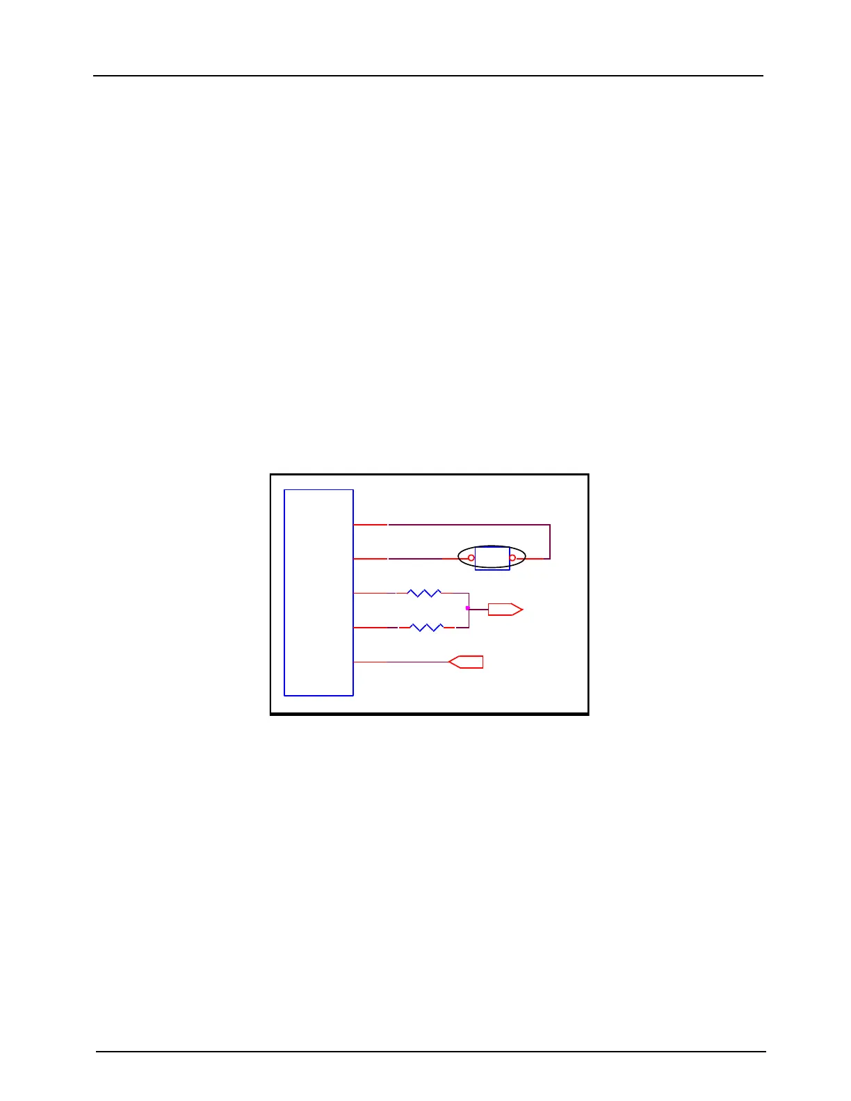
U1
CH 7511B
ENAVDD
47
IRQ
36
PWM_OUT0
48
PWM_OUT1
39
PWM_IN
49
JP1
HEADER 1x2
1 2
R1 0
R2 0
PWM_OUT
PWM_IN
Figure 12: PWM and IRQ Control connections
• IRQ
IRQ (pin 36) can output an interrupt signal when the BLUP and BLDN are executing and should be connected to
ENAVDD pin as shown in Figure 12.
• Reserved
Reserved pin (pin 2) should be left open in the application.
2.8 Important Design Considerations
(Panel power, backlight power, pull-up voltage)
• LVDS Power
Close attention must be paid to the power supplied to the LVDS backlight and the LVDS panel. Power requirements
may differ from panel to panel. Please check the panels’ power and backlight voltage specifications. The ENABKL
and ENAVDD may be used to control the power for the LVDS backlight and the LVDS logic circuitry.
 Loading...