CHRONTEL AN-B014
206-1000-014 Rev. 1.7 2020-07-14 11
• Signal Wires, POWER and GND layout
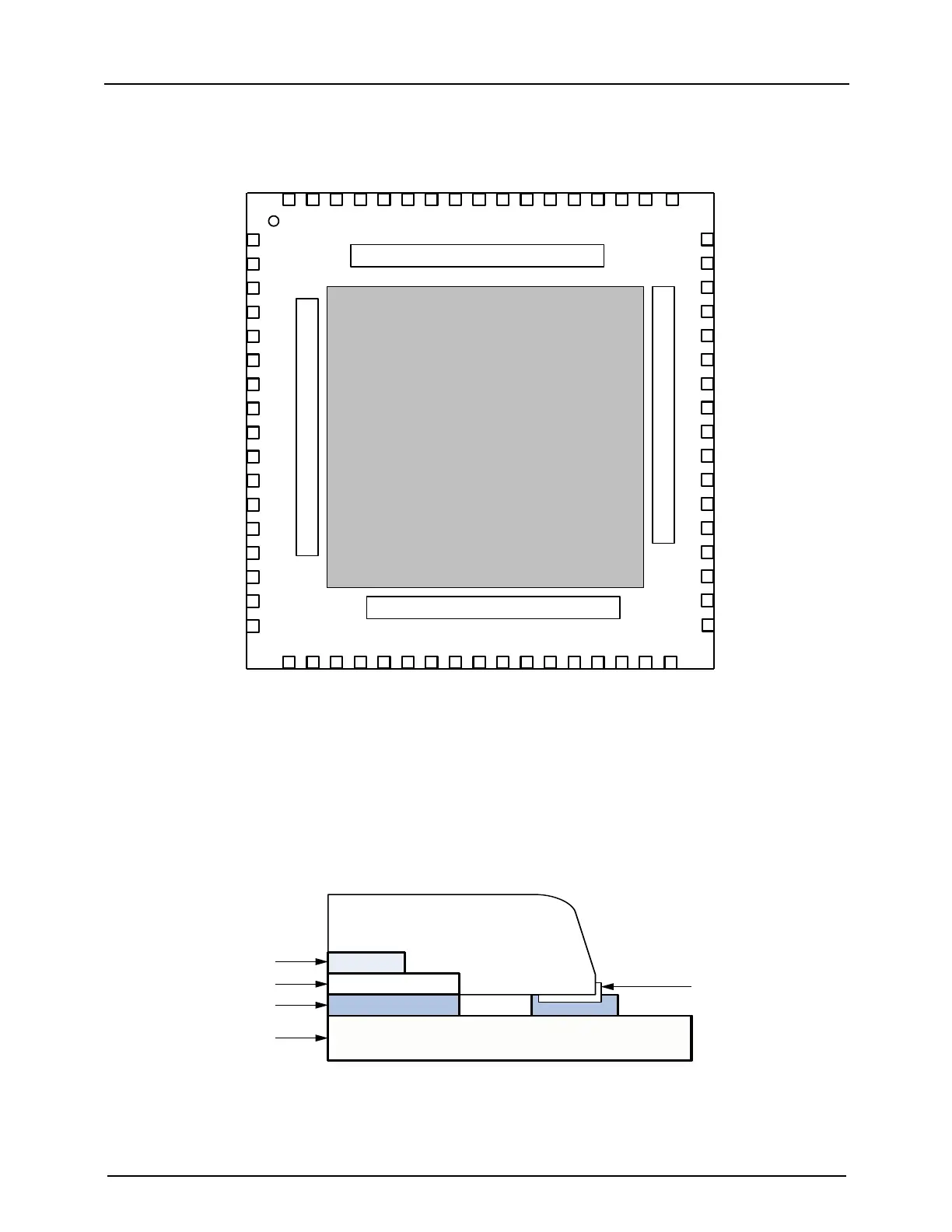
Do not layout the wire or VIAs between the exposed thermal pad and the pin pads. Refer to Figure 13.
1
2
3
4
5
6
7
8
9
10
11
12
13
14
15
16
17
18
19
20
21
22
23
24
36
35
34
48
47
46
45
44
43
42
41
40
39
38
37
25
26
27
28
29
32
31
30
64
63
62
61
60
59
58
57
56
55
54
53
52
49
50
51
33
65
66
67
68
Thermal exposed pad
Figure 13: Wires or vias are not allowed in these four areas
2.9 Thermal Exposed Pad Package
The CH7511B/7512B is available in a 68-pin QFN package with exposed thermal pad. The advantage of the exposed
thermal pad package is that the heat can be dissipated through the ground layer of the PCB more efficiently. When
properly implemented, the exposed thermal pad package provides a means of reducing the thermal resistance of the
CH7511B/7512B. Careful attention to the design of the PCB layout is required for good thermal performance. For
maximum heat dissipation, the exposed thermal pad of the package should be soldered to the PCB as shown in Figure
14.
Die
Exposed Pad
Solder
PCB
Pin
Figure 14: Cross-section of exposed thermal pad package
 Loading...