CHRONTEL AN-B014
206-1000-014 Rev. 1.7 2020-07-14 9
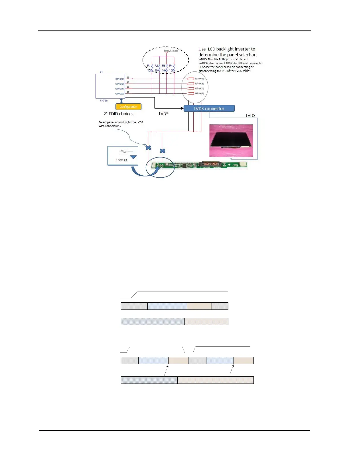
Figure 10: Typical application to control the CH7511B/7512B GPIO[3:0]
Method 2
GPIO [3:0] can be controlled by another chip’s GPIO pins in the CH7511B/7512B application system. If the chip
controlling the CH7511B/7512B GPIO [3:0] cannot set the expected value before the CH7511B/7512B finishes
loading its firmware (typically 100ms after the CH7511B/7512B is powered ON), the controlling chip must reset the
CH7511B/7512B for it to load the Boot ROM file again. It is recommended that the CH7511B/7512B be reset by the
controlling chip each time the LVDS Panel selection value is changed.
Figure 11 shows the typical cases to control the CH7511B/7512B GPIO [3:0] by another chip. Case 1 is the right
loading case, in which the GPIO pins remains stable within 100ms after reset. Case 2 is the wrong loading case, in
which the GPIO value, represented by the GPIO pins, is still at random after the firmware is completely loaded.
Therefore, the reset signal must be given again. The reset pulse width of larger than 10ms is recommended.
RESETB
Loading FirmwareIDLE
Loading LVDS
Configurations
CH7511 I2C
Master Activity
Random Values
Correct LVDS Panel Selection Value
IDLE
CH7511 GPIO[3:0]
Case 1: CH7511 GPIO[3:0] settles before it starts loading LVDS configurations
RESETB
Loading Firmware
IDLE
Loading LVDS
Configurations
CH7511 I2C
Master Activity
Random Values
Correct LVDS Panel Selection Value
IDLE
CH7511 GPIO[3:0]
Case 2: CH7511 GPIO[3:0] cannot settle before it starts loading LVDS configurations
Loading Firmware
Loading LVDS
Configurations
Wrong LVDS
configurations!
Correct LVDS
configurations!
Reset pulse generated by
Customers host chip
Figure 11: Typical cases to control CH7511B/7512B GPIO [3:0] by host chip
 Loading...