CHRONTEL AN-B014
4 206-1000-014 Rev. 1.7 2020-07-14
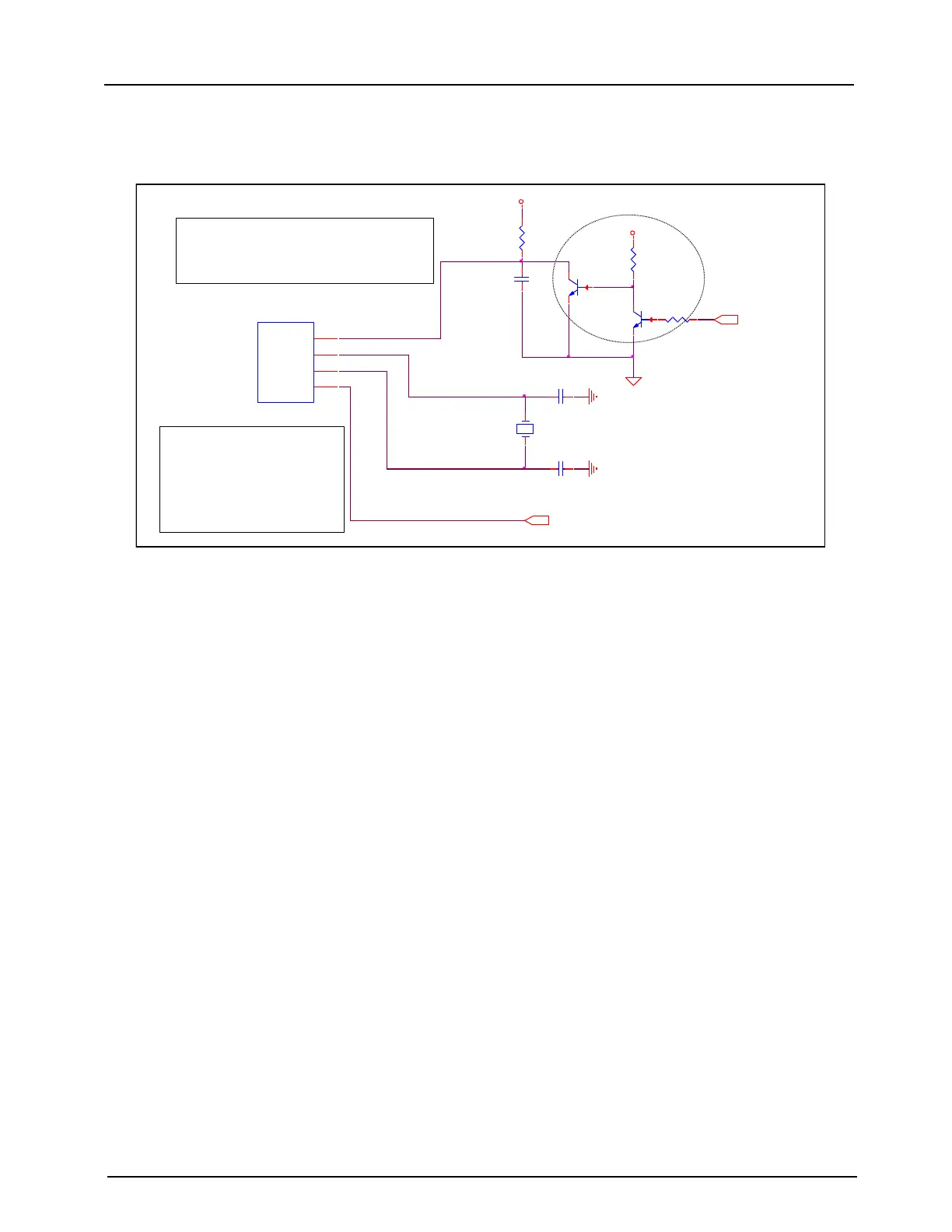
The REFCK is another optional pin as the reference input clock for the CH7511B/7512B. A 27MHz (3.3V) clock
may be injected at this pin as shown in Figure 3. For PCB design, the capacitor must be placed as close as possible to
the REFCK pin, with traces connected from point to point, overlaying the ground plane.
U1
CH7511B
RESETB
1
XI
6
XO
5
REFCK
9
Note: The resetb is 1.8V level.
It need 10Kohm resister to 1.8V
and 0.1uf capacitor to GND.
So if the system reset signal is 3.3V,
the level shift circuit is necessary.
R3
1k
R2
10K
VCC33
RESETB_PCH
R1
10K
Q2
PMBS3904
1
2 3
Q1
PMBS3904
1
2 3
C1
0.1uF
12
VCC18
RESETB
C2
22pF
Y1
27MHz
C3
22pF
REFCK
NOTE: CH7511B supports two
kinds of clock input ways
Option1: us e 27MHz crys tal with 22pf
capacitors
Option 2: inject clock 27MHz (3.3V) in
REFCK pin(Pin 9)
Custom er must choose one option
for CH7511B clock
Figure 3: General Control Pins
2.4 Serial Port Control Pins
• SPC0 and SPD0
SPD0 and SPC0 function as a serial interface where SPD0 is the bi-directional data and SPC0 is an input-only serial
clock. In the reference design, SPD0 and SPC0 pins are pulled up to LVDD (+3.3V) with 6.8k resistors. Through
these two pins, the internal register values of the chip can be read. The external Boot ROM can be updated if these
pins are connected to SPC1 and SPD1 with jumpers as shown in Figure 4.
• SPC1 and SPD1
SPD1 and SPC1 function as a serial interface where SPD1 is bi-directional data and SPC1 is an input only serial clock.
In the reference design, SPD1 and SPC1 pins are pulled up to LVDD (+3.3V) with 6.8kΩ resistors as shown in Figure
4.
SPD1 and SPC1 are used to interface with the CH9904 (the serial Boot ROM). The CH7511B/7512B will auto-load
the values, such as EDIDs and configurations, etc., from the Boot ROM upon power-on or reset.
 Loading...