CHRONTEL AN-B014
206-1000-014 Rev. 1.7 2020-07-14 5
U1
CH7511B
SPC0
54
SPC1
51
SPD0
53
SPD1
50
SPC0
R2
6.8K
1 2
R1
6.8K
1 2
VCC3_3
SPD0
R6
6.8K
R5
6.8K
R810K
R4
6.8K
1 2
U2
CH9904
GP1
1
GP2
2
GP3
3
GND
4
SPD
5
SPC
6
WE
7
VCC
8
R3
6.8K
1 2
VCC3_3VCC3_3VCC3_3
R7
6.8K
SPD1
SPC1
JP1
HEADER 1x2
1 2
JP2
HEADER 1x2
1 2
SPD0
SPC1SPC0
SPD1
CH7511B Boot Rom
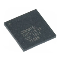
Figure 4: Serial Port Control
Note:
If you use SPC0/SPD0 or the AUX channel to update the CH9904 Boot ROM, the precondition is that
the MCU firmware must work properly. It is recommended that the IIC/SMBUS be used to update
CH9904, by linking the IIC/SMBUS to SPC0 and SPD0
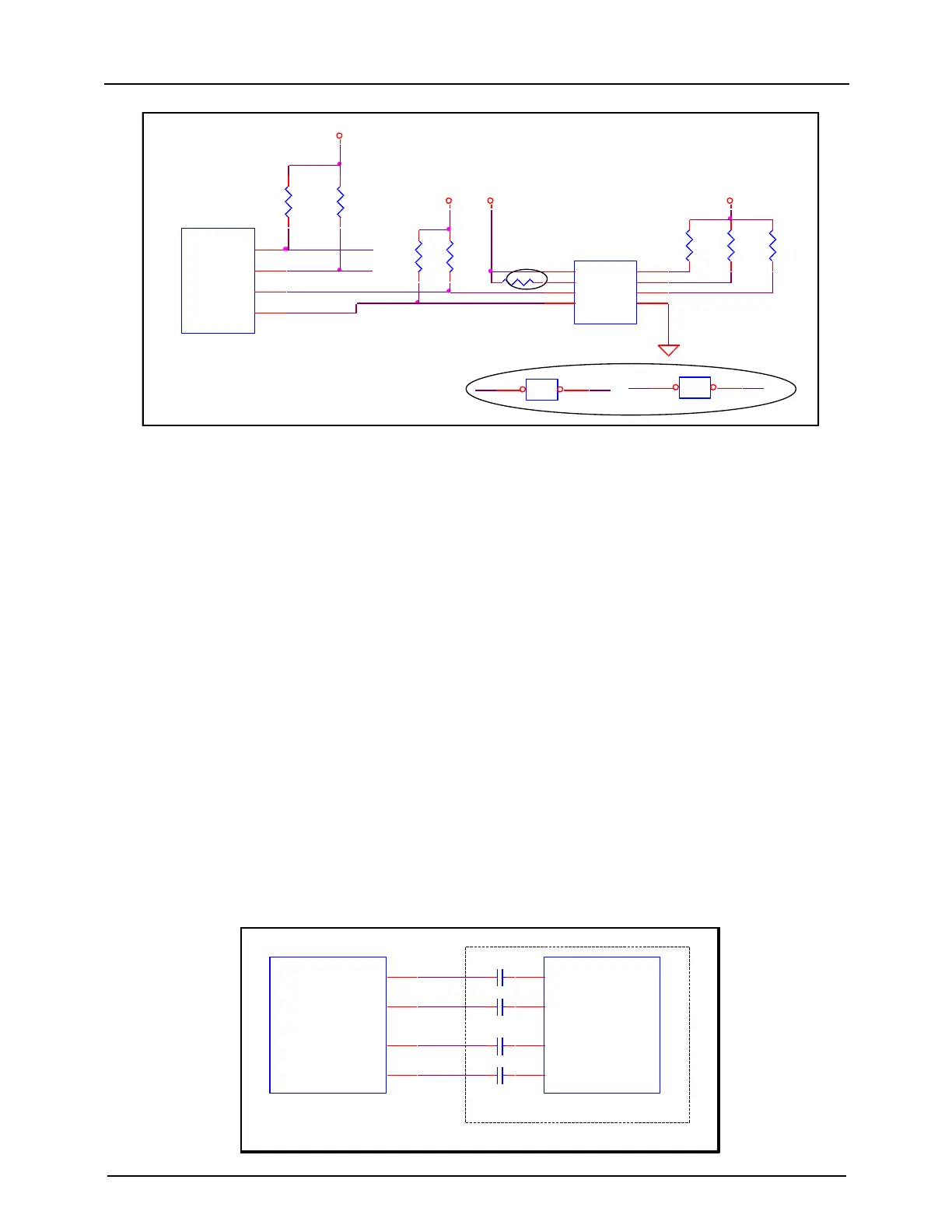
2.5 Display Port Signal Pins
• DP0P/N, DP1P/N
These pins accept two AC-coupled differential pair signals from the Display Port transmitter.
Since the digital serial data of the CH7511B/7512B may be toggled at speeds up to 2.7 GHz, it is strongly
recommended that the connection of these video signals between the graphics controller and the CH7511B/7512B be
kept as short as possible, avoid discontinuities in the reference plane and be isolated as much as possible from the
analog outputs and analog circuitry. For optimal performance, these signals should not overlay the analog power or
analog output signals. When a signal pair has to changes layers, the ground stitching vias should be placed close to
the signal vias. A minimum of 1 to 3 stitching vias per pair of signals is recommended. Never route a trace so that it
straddles a plane split. It is recommended that 5 mils traces be used in routing these signals. There should be 7 mils
spacing between each intra pair. The length for a pair of intra differential signals should be matched within 5 mils.
The length for inter pairs should be matched within 2 inches. Bend smaller than 45 degrees should be avoided. The
AC coupling capacitors for the serial video inputs must be placed close to the GMCH, as shown in Figure 5.
GMCHCH7511
C1 0.1uF
C2 0.1uF
C3 0.1uF
C4 0.1uF
Source
DP0P
61
DP0N
62
DP1P
64
DP1N
65
DP0P
DP0N
DP1P
DP1N
 Loading...