CHRONTEL AN-B014
6 206-1000-014 Rev. 1.7 2020-07-14
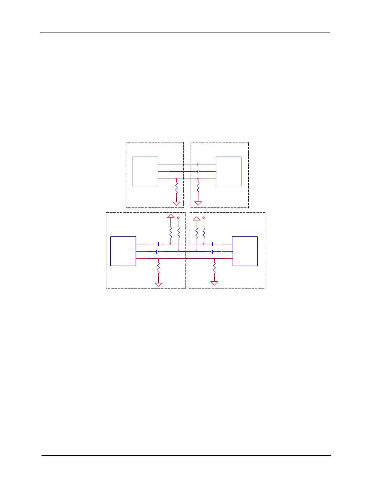
Figure 5: CH7511B/7512B DP Main Link Lane Inputs
• AUXP and AUXN
These two pins are for Display Port AUX channel control that accepts a half-duplex, bi-directional AC-coupled
differential signal. An AC coupling capacitor, 0.1uF recommended, must be placed on the end as shown in Figure 6.
• HPDET
This output pin indicates whether the device is active or not. It also generates an interrupt pulse as defined by the
Display Port standard. Output voltage is 3.3V. A resistor, greater than 100KΩ, should be connected between this pin
and GND as shown in Figure 6.
U1
CH 7511B
AUXN
43
HPDET
59
AUXP
44
U2
GMCH
AUXN
HPDET
AUXP
C1 0.1uF
C2 0.1uF
R1
100K
R2
100K
Sink Source eDP
U3
CH 7512B
AUXN
43
HPDET
59
AUXP
44
U4
GMCH
AUXN
HPDET
AUXP
C3 0.1uF
C4 0.1uF
R3
100K
R4
100K
Source DP
Sink
C5 0.1uF
C6 0.1uF
R5
1M
R6
1M
R7
100K
R8
100K
+3.3V +3.3V
Figure 6: CH7511B/7512B AUX channel and HPDET
2.6 LVDS Signal Pins
• LVDS Outputs (LDCxP and LDCxN)
The LVDS output signals are LDCxP and LDCxN. The LVDS is a differential interface with a nominal swing 200mV.
The following rules should be applied to the signals:
1. Keep traces as short as possible.
2. Make these traces have 100Ω differential impedance.
3. Trace widths should be 5 mils.
4. Intra Pair spacing (spacing between the “+” and “-” pairs) should be 7mils.
5. Inter Pair spacing (spacing between one differential pair and another) should be a minimum of 20 mils
except in the area near the pins.
6. Difference in trace lengths between “+” and “-” pairs should be within 5mils.
7. Difference in trace lengths among Inter pairs should be within 10mils.
8. “+” And “-” pairs should be routed in parallel.
2.7 Other function pins
 Loading...