-6-
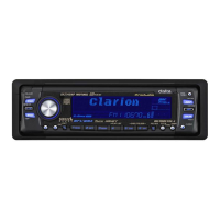
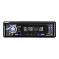
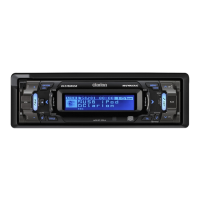
DXZ745MP/DXZ746MP
M30622MWP-128GP 052-3934-00 Main System controller
1. Terminal Description
EXPLANATION OF IC
Main section
CD mechanism section: 929-0300-82
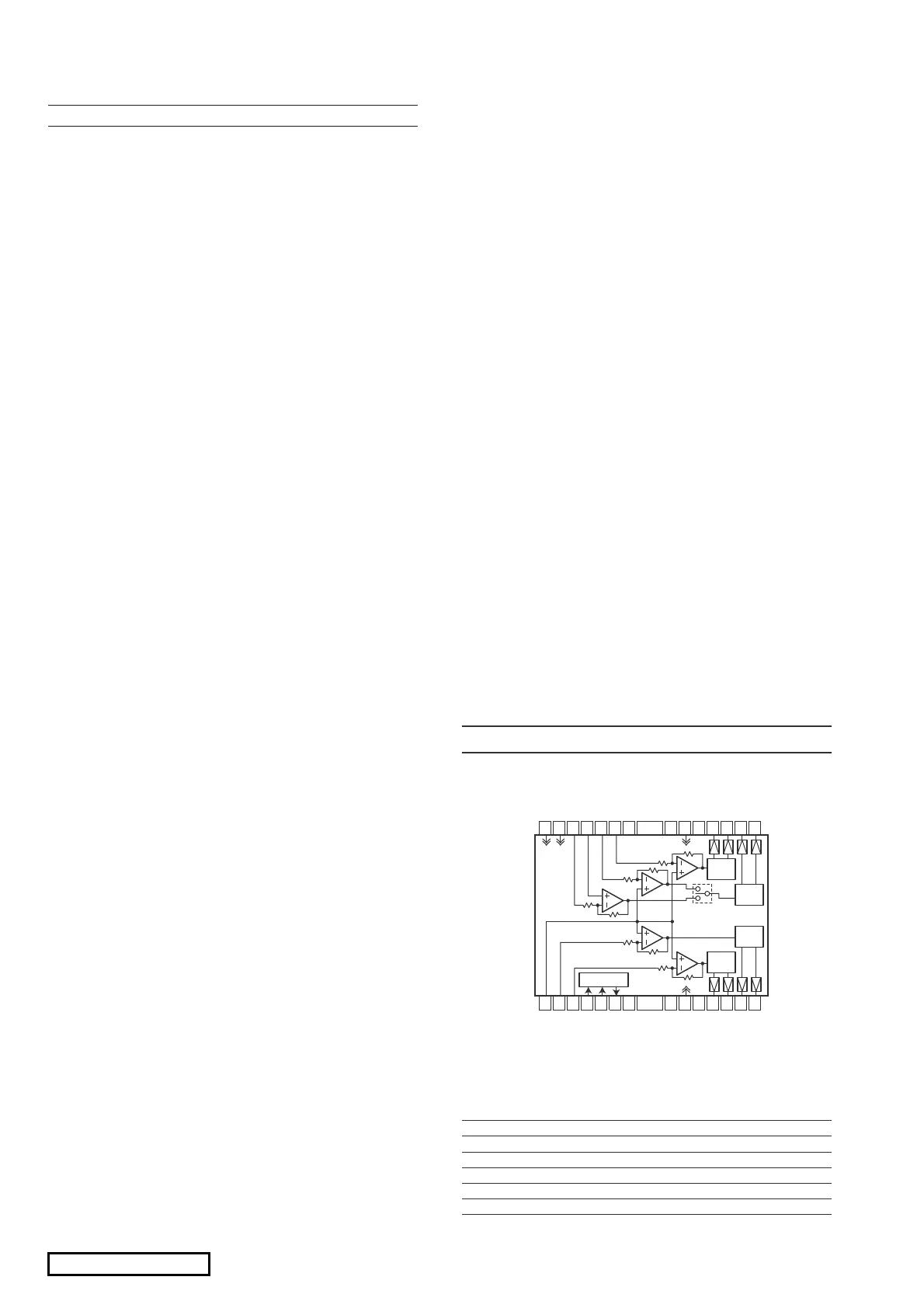
051-6069-08 FAN8047G3 4 channel Motor Driver
Function Table
SW45 Mute1,2_ Mute 3_ Mute 4_ 1 ch 2 ch 3 ch 4 ch
in in in in out out out out
(pin 28) (pin 9) (pin 27) (pin 20) (pin13,14) (pin11,12) (pin17,18) (pin15,16)
H H H x ON ON ON ON A
H H L x ON ON OFF ON A
H L H x OFF OFF ON OFF
H L L x OFF OFF OFF OFF
L x x H OFF OFF OFF ON B
L x x L OFF OFF OFF OFF
1
2
3
4
5
6
7
8
9
10
11
12
13
14
Level
Shift
Level
Shift
28
27
26
25
24
23
22
21
20
19
18
17
16
15
Level
Shift
Level
Shift
Vref 1
1 ch in
2 ch in
Reg on(H)
Reg feed
Reg out
Ground
P Vcc 1
Mute 1,2_
Ground
2 ch out -
2 ch out +
1 ch out -
1 ch out +
SW 45
Mute 3_
4 ch in B
Vref 2
4 ch in A
3 ch in
S Vcc
P Vcc
Mute 4_
Ground
3 ch out-
3 ch out+
4 ch out-
4 ch out+
Regulator
pin 1
CONTRAST-CONT
O
Contrast controller
pin 2
TIME BASE
IN
Time base pulse input.
pin 3
REMOCON
IN
Remote controller signal input terminal.
pin 4
2-Z MUTE
O
2-ZONE mute.
pin 5
NU
IN
Not in use.
pin 6
BYTE
IN
The data length selection(8bit/16bit).
pin 7
CN VSS
IN
Connect to VSS.
pin 8
JOG-CW
IN
Jog key signal input.
pin 9
JOG-CCW
IN
Jog key signal input.
pin 10
RESET
IN
Reset signal input.
pin 11
X-OUT
O
Crystal connection.
pin 12
VSS
-
Negative supply voltage.
pin 13
X-IN
IN
Crystal connection.
pin 14
VCC
-
Positive supply voltage.
pin 15
NU
IN
Not in use.
pin 16
ACC_DET
IN
ACC detection signal input.
pin 17
B/U_DET
IN
Backup detection signal input.
pin 18
KEY_INT
IN
Key interrupting signal input.
pin 19
27pin CONNECT
IN
Connect to 27pin.
pin 20
MOTOR+ O
The control signal output to the motor.
pin 21
MOTOR-
O
The control signal output to the motor.
pin 22
SUB_0BIT_MUTE
O
CD ON signal output.
pin 23
E_VOL CLK1
O
Mitsubishi electric volume IC M15623FP
serial signal output.
pin 24
E_VOL DATA1
O
Mitsubishi electric volume IC M15623FP
serial signal output.
pin 25
CATS_ LED
O
CATS LED drive output.
pin 26
NU
IN
Not in use.
pin 27
IE BUS RX
IN
IE Bus serial data input.
pin 28
IE BUS TX
O
IE Bus serial data output.
pin 29
NU
O
Not in use.
pin 30
NU
IN
Not in use.
pin 31
NU
IN
Not in use.
pin 32
NU
O
Not in use.
pin 33
LCD SO
O
The serial data output to the LCD driver.
pin 34
LCD SI
IN
The serial data input from the LCD driver.
pin 35
LCD CLK
O
The clock pulse output to the LCD driver.
pin 36
LCD KEY REQ
IN
LCD Key request signal output.
pin 37
LCD CS
O
Chip select signal output to LCD.
pin 38
DIR CSN
O
The chip select signal to DIR IC.
pin 39
NU
IN
Not in use.
pin 40
MP3 SRQ
IN
MP3 request signal input.
pin 41
MP3 CS
O
MP3 chip selection signal output.
pin 42
MP3 WP
O
MP3 wakeup signal output.
pin 43
MP3 RESET
O
MP3 reset signal output.
pin 44
E/INT
IN
The emphasis data input for the
digital-audio-interface-receiver.
pin 45
INIT 1 IN
The initial setting input.
pin 46
MAIN_0Bit_MUTE
O
When main zone, CD mode the port HI.
pin 47
FIL CONT 1
O
The cut off control signal output to the filter.
pin 48
FIL CONT 2
O
The cut off control signal output to the filter.
pin 49
PLL CE
O
The chip enable signal output to the PLL IC.
pin 50
PLL SCK
O
The clock pulse output to the PLL IC.
pin 51
PLL SI
IN
Serial data input from the PLL IC.
pin 52
PLL SO
O
Serial data output to the PLL IC.
pin 53
VARI SCL
O
Variable color clock output.
pin 54
VARI SDA
O
Variable color serial data output.
pin 55
DIR CLK
O
DIR-IC serial clock signal.
pin 56
DIR DATA
O
DIR-IC serial DATA signal input.
pin 57
DIG RESET
O
The reset pulse output.
pin 58
DAC DATA
O
The serial data output to DAC.
pin 59
DAC CLK
O
The clock pulse output to DAC.
pin 60
VCC
-
Positive supply voltage.
pin 61
DAC _CSN
O
The chip select signal output to DAC.
pin 62
VSS
-
Negative supply voltage.
pin 63
OPEN POSI
IN
The open position detect signal input.
pin 64
NU
IN
Not in use.
pin 65
ST/SD
IN
At receiving the FM station, this port detects the
stereo signal. At seeking or scanning, this port
detects the station detection signal.
pin 66
NU
O
Not in use.
pin 67
NU
O
Not in use.
pin 68
NU
O
Not in use.
pin 69
NU
O
Not in use.
pin 70
NU
IN
Not in use.
pin 71
OFFSET DET
IN
The emergency signal input from the power IC.
pin 72
DIG 5V
O
The ON signal output to the power supply section.
pin 73
NU
IN
Not in use.
pin 74
E-VOL CLK2
O
Clock pulse output to the volume IC. (M61508FP)
pin 75
E-VOL DATA2
O
The serial data output to the volume IC. (M61508FP)
pin 76
CLOSE POSI
IN
The close position detect signal input.
pin 77
NU
O
Not in use.
pin 78
AMP MUTE
O
Muting signal output to the Audio Power Amplifier.
pin 79
NU
O
Not in use.
pin 80
SYS MUTE
O
System muting signal output.
pin 81
PHONE INT
IN
The telephone interrupt signal input.
pin 82
ILLUMI DET
IN
Illumination ON signal input.
pin 83
AMP-REMDET
IN
Remote controller wire short detection.
pin 84
EX-AMPREM
O
Extra audio power amplifier.
pin 85
AUTO ANT
O
Motor antenna control signal output.
pin 86
5V REM
O
ON signal output to the 5V power supply.
pin 87
NU
IN
Not in use.
pin 88
NU
IN
Not in use.
pin 89
KEY A/D
IN
Input terminal of A/D converter for Key judgment.
pin 90
NU
IN
Not in use.
pin 91
DISP5V_REM
O
The ON signal output to the power supply section.
pin 92
INT-AMPREM
O
The control signal output to internal audio power
amplifier.
pin 93
SYS ACC
O
ACC detect signal output.
pin 94
A VSS
-
Analog ground.
pin 95
NU
IN
Not in use.
pin 96
VREF
IN
Reference voltage.
pin 97
A VCC
-
Positive supply voltage for the internal analog
section.
pin 98
MP3 SI
IN
MP3 serial data input.
pin 99
MP3 SO
O
MP3 serial data output.
pin100
MP3 SCK
O
MP3 clock output.
 Loading...