5
5
4
4
3
3
2
2
1
1
D D
C C
B B
A A
M/B USB
port0(2.0+3.0)
TYPE-C
M/B USB
port1(2.0+3.0)
TYPE-A
M/B USB port0(2.0+3.0)
TYPE-C
M/B USB port1(2.0+3.0)
TYPE-A
AMI Debug Use
TP
㓦
㓦㓦
㓦⛐
⛐⛐
⛐ᶨ
ᶨᶨ
ᶨ崟
崟崟
崟
㓦
㓦㓦
㓦⛐
⛐⛐
⛐
BOT
Hardware Straps (3)
Internal PD 20K CMOS
Internal PD 20K CMOS
Enable CSE ROM Bypass
1=enable bypass
0=disable bypass (default)
Force DNX FW Load
1=Force
0=Do not force (default)
Internal PD 20K CMOS
GPIO_40,48
Please ensure that this strap is pulled LOW when
RSM_RST_N de-asserts for normal platform operation.
Internal PD 20K CMOS
Internal PU 20K CMOS
Allow eMMC as a boot source
1=enable (default)
0=disable
Internal PU 20K CMOS
Allow SPI as a boot source
1=enable (default)
0=disable
CCD port 6
BT port 7
M/B 3G/LTE port3
U/B USB port4 (2.0)
U/B USB port2 (2.0)
3G / LTE
Internal PD 20K CMOS
When the platform does not use the
USB2_OTG_ID and USB2_VBUS_SNS pins,
USB2_OTG_ID pin should be unconnected on
the platform (terminated with internal
pull ups] and USB2_VBUS_SNS should be
connected to ground.
0421 DEL test pad
0428 Modify net
0428 Modify Value
0621 modify R672,R673
0801 Add"*"
0726 Modify port 5 to 2
USB_OC#01
USB_OC#0
USB_RCOMP
USB_VBUSSNS
SSIC_RCOMP
SOC_GPIO43
UART1_RXD
SOC_GPIO44
UART_RXD_Q
UART_TXD_QUART1_TXDSOC_GPIO43
UART1_RXD
SOC_GPIO47
UART2_RXD
SOC_GPIO49
SOC_GPIO48
UART2_TXDSOC_GPIO47
UART2_RXD
SOC_GPIO47
SOC_GPIO48
SOC_GPIO39
SOC_GPIO40
SOC_GPIO43
SOC_GPIO44
USB_OTG_ID
EMMC_R ST#
SOC_GPIO40
SOC_GPIO39
SOC_GPIO49
1.8VA
3.3VA1.8VA
1.8VA
1.8VA
USB_PN0 24
USB_PP0 24
USB_PN1 18
USB_PP1 18
USB3_TX0_P24
USB3_TX0_N24
USB3_RX0_P24
USB3_RX0_N24
USB3_RX1_P18
USB3_RX1_N18
USB3_TX1_N18
USB3_TX1_P18
USB_PP619
USB_PN619
USB_PP720
USB_PN720
USB_PN3 20
USB_PP3 20
USB_PN2 19
USB_PP2 19
USB_PN4 19
USB_PP4 19
USB3_TX3_N20
USB3_TX3_P20
USB3_RX3_N20
USB3_RX3_P20
SMI#_N 37
EMMC_R ST#10
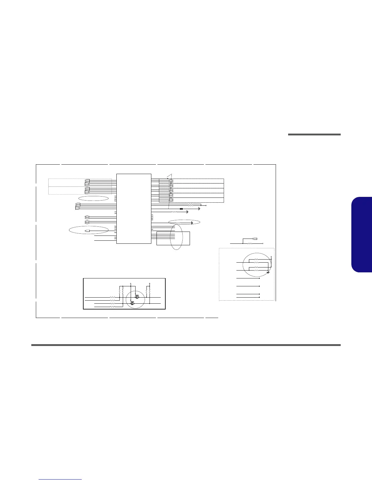
Title
Size
Document Number R e v
Date: Sheet
of
6-71-N24P0-D02
2.0
[06] APL SOC_5/8_USB,GPIO
B
639Friday, August 05, 2016
ᙔ!Ϻ!ႝ!တ!!DMFWP!DP/
Title
Size
Document Number R e v
Date: Sheet
of
6-71-N24P0-D02
2.0
[06] APL SOC_5/8_USB,GPIO
B
639Friday, August 05, 2016
ᙔ!Ϻ!ႝ!တ!!DMFWP!DP/
Title
Size
Document Number R e v
Date: Sheet
of
6-71-N24P0-D02
2.0
[06] APL SOC_5/8_USB,GPIO
B
639Friday, August 05, 2016
ᙔ!Ϻ!ႝ!တ!!DMFWP!DP/
R677
*2.2K_04
R671 137_1%_04
R683 *0_04
APL_SOC
USB3.0
USB2.0
HSIC
UART
6 OF 13
REV = 0.7
U25F
USB3_TXP1
K3
USB_DN2
V13
USB_DN3
V7
USB_RCOMP
Y15
GPIO43/UART1_TXD
B43
GPIO42/UART1_RXD
C43
GPIO45/UART1_CTS_B
C42
GPIO44/UART1_RTS_B
A42
USB3_TXP0
J1
USB_DP4
Y9
USB_DN0
V10
USB_DN1
V15
USB_VBUSSNS
AC16
USB_OTG_ID
AC15
USB3_TXN0
J2
USB3_TXN1
K2
PCIE_TXP5/USB3_T XP2
L2
USB_DN4
Y10
USB_DP2
Y13
USB_DP0
V12
USB_DP1
V16
USB_DP3
V9
USB3_RXN0
K10
USB3_RXN1
G2
USB3_RXP0
K9
USB3_RXP1
F2
USB_SSIC_0_RXP
AG16
USB_SSIC_0_TXP
AH13
USB_SSIC_0_RXN
AG15
USB_SSIC_0_TXN
AH12
USB_SSIC_RCOMP
AB15
USB_OC0_N
B55
USB_OC1_N
C55
GPIO48/UART2_RTS_N
L41
GPIO49/UART2_CTS_N
M41
GPIO47/UART2_TXD
H41
GPIO46/UART2_RXD
J41
PCIE_TXN5/USB3_TXN2
L1
PCIE_RXP5/USB3_RXP2
K7
PCIE_RXN5/USB3_RXN2
M7
PCIE_TXP4/USB3_T XP3
N2
PCIE_TXN4/USB3_TXN3
M2
PCIE_RXP4/USB3_RXP3
H5
PCIE_RXN4/USB3_RXN3
H6
GPIO39/UART0_TXD
B45
GPIO38/UART0_RXD
C45
GPIO41/UART0_CTS_N
C44
GPIO40/UART0_RTS_N
A46
USB_DP5
AB6
USB_DN5
AB7
USB_DP6
AC12
USB_DN6
AC10
USB_DP7
V5
USB_DN7
V6
GPIO216/JTAG_TCK
P30
GPIO217/JTAG_TDI
M29
GPIO218/JTAG_TMS
M30
GPIO219/JTAG_TDO
L30
PCH_JTAGX
B21
R676
*2.2K_04
R668 10K_04
S
D
G
Q46A
*MTDK3S6R
2
61
S
D
G
Q46B
*MTDK3S6R
5
34
R670 *20mil_short_04
R448 113_1%_04
R675 *4.7K_04
eMMC
R678
*10K_04
R669 10K_04
R679
*10K_04
R672 *4.7K_04
eMMC
R682 *0_04
R152 *4.7K_1%_04
R673 4.7K_04
eMMC
R674 *4.7K_04
W/O e MMC
R680 *0_04
R681 *0_04