Do you have a question about the Clevo NP50HH and is the answer not in the manual?
Legal and revision information regarding the publication and its contents.
List of registered trademarks mentioned in the manual.
Describes the manual's purpose, scope, intended audience, and content structure.
Critical safety precautions to reduce risk of fire, electric shock, and injury.
Regulatory compliance information regarding FCC rules and interference.
Guidelines for proper notebook care to prevent damage and ensure longevity.
Advice on keeping the computer away from electromagnetic interference.
Recommendations for using external peripheral devices with the notebook.
Essential safety guidelines related to the notebook's power adapter and usage.
Important guidelines for safe battery handling, charging, and disposal.
Best practices for battery usage, storage, and maintenance.
Information on proper and legal disposal of rechargeable batteries.
References to other manuals or documentation for additional information.
Step-by-step instructions for initial computer setup and power on.
Correct procedure for safely shutting down the operating system and computer.
Provides a general description of the manual's scope and content.
Detailed technical specifications of the notebook hardware components.
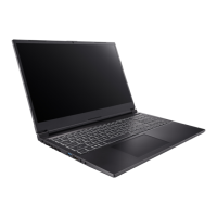
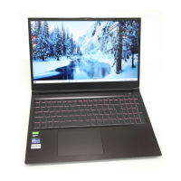
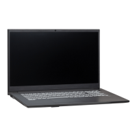
Identifies components on the top view of the notebook with the LCD panel open.
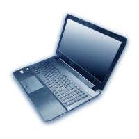
Identifies components on the front and right side views of the notebook.
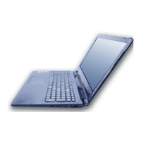
Identifies components on the left side and rear views of the notebook.
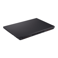
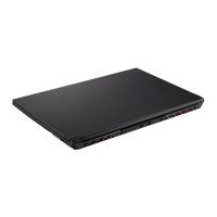
Identifies components visible on the bottom of the notebook.
Highlights key components located on the top side of the mainboard.
Highlights key components located on the bottom side of the mainboard.
Identifies and labels connectors on the top side of the mainboard.
Identifies and labels connectors on the bottom side of the mainboard.
General information about the disassembly procedures and reassembly guidance.
Lists the recommended tools required for performing disassembly tasks.
Describes different types of computer connectors and how to handle them.
Crucial safety and handling precautions to prevent damage and injury during maintenance.
Provides guidelines and instructions for cleaning the notebook's exterior and interior.
Provides a structured list of disassembly procedures for various components.
Detailed step-by-step instructions for removing the keyboard assembly.
Step-by-step instructions for safely removing the notebook's battery.
Guide for safely removing the M.2 Solid State Drive module.
Instructions for removing the notebook's hard disk drive.
Guide for removing and replacing RAM modules in the system.
Step-by-step instructions for removing the Wireless LAN module.
Information on color coding for WLAN antenna cables for identification.
Step-by-step instructions for installing the touchpad assembly.
Indicates the page numbers for finding illustrations of various part lists.
Illustrations and part numbers for the top assembly of specific notebook models.
Illustrations and part numbers for the top assembly of specific notebook models.
Part list illustrations and component numbers for the bottom assembly.
Part list illustrations and component numbers for the main logic board.
Part list illustrations and component numbers for the Hard Disk Drive assembly.
Part list illustrations and component numbers for the LCD panel assembly.
Part list illustrations and component numbers for the LCD panel assembly.
Index of schematic diagrams with corresponding page numbers.
High-level overview of the system's architecture and major component interactions.
Detailed schematic of processor interface signals like DMI, PEG, and display interfaces.
Detailed schematic of processor DDR4 memory interface signals.
Detailed schematic of processor clock, JTAG, and miscellaneous control signals.
Detailed schematic of processor power delivery rails and control signals.
Detailed schematic of processor power delivery network, focusing on specific voltage rails.
Detailed schematic showing processor power and ground pin assignments.
Schematic diagram illustrating the DDR4 memory interface for Channel A.
Schematic diagram illustrating the DDR4 memory interface for Channel B.
Schematic detailing the VGA's PCI Express interface connections.
Schematic showing the GPU's frame buffer memory partitioning configuration.
Detailed schematic of the GPU frame buffer A interface signals.
Detailed schematic of the GPU frame buffer B interface signals.
Schematic illustrating the coupling capacitors for the VGA NVVDD power rail.
Schematics related to system configuration straps and crystal oscillator circuits.
Schematic for the IFP (Internal Flexible Port) I/O interface connections.
Schematics for miscellaneous GPIO pins, I2C bus, and VBIOS related connections.
Diagram illustrating the power-up sequence for NVIDIA GPU components.
Schematic showing the GPU NVVDD and FBVDDQ power delivery network.
Schematic diagram illustrating the ground connections for the GPU.
Schematic for the Mini DisplayPort interface, including signal routing.
Schematics for the LCD panel connector and backlight inverter circuitry.
Schematic diagram for the HDMI interface, including TMDS signals.
Detailed schematic of PCH interfaces: SPI, SMBus, and USB connections.
Detailed schematic of PCH interfaces: DMI, PCIe, and RTC signals.
Detailed schematic of PCH interfaces: SATA, Host, and HDA connections.
Detailed schematic of PCH interfaces: SMBus, ESPI, and UART connections.
Detailed schematic of PCH clock outputs and CNVI interface signals.
Detailed schematic illustrating the PCH power rails and their distribution.
Detailed schematic showing PCH ground connections and miscellaneous pins.
Schematic diagram of the ALC256 audio codec and its peripheral connections.
Schematics for the M.2 interface supporting WLAN, Bluetooth, and PCIe SSDs.
Schematics for the USB Type-C and Type-A ports, including charger functionality.
Schematic diagram for the RTS5227S card reader interface.
Schematic for the RTL8111H Gigabit LAN controller and its connections.
Schematics for HDD, touchpad click pad, and audio board connections.
Schematics for the LED indicators, CCD/DMIC, TPM, and power switch board.
Schematic diagram for the IT5570 Keyboard Controller (KBC) and related functions.
Schematic diagram detailing the RGB Keyboard illumination and control signals.
Schematics showing the VDD3 and VDD5 power rail generation and distribution.
Schematics for 1.8V, NV3V3, and 3.3VA power rails and their control.
Schematics for 3V, 5V, 3VS, and 5VS power rail generation.
Schematics for 1.8V, 1.8VS, 1.8VA, and C10 power rails.
Schematics illustrating the VCCST and VCCSTG power rails.
Schematics for the VNN and V1.05 power rails.
Schematic diagram of the VCCIN power rail and its control signals.
Schematics detailing the output stages of the VCCIN power rail.
Schematic for the AC input jack and battery charging control circuitry.
Schematic diagram of the VCCIN AUX power rail and its associated components.
Schematics for the DDR memory power rails at 1.2V, 0.6V, and 2.5V.
Schematic diagram for the NVVDD1 power rail and its driver circuitry.
Schematic diagram for the NVVDD2 power rail and its driver circuitry.
Schematic diagram for the PEX_VDD power rail and its associated components.
Schematic diagram for the FBVDDQ power rail and its driver circuitry.
Schematic for Over Voltage Measurement (OVRM) and related monitoring circuits.
Schematics for the audio board components and redriver circuitry.
Schematic diagram illustrating the connections and functionality of the LED indicators.
Schematic diagram for the power switch board and its associated buttons.
Schematic diagram for the 17-inch LED board components.
Diagram illustrating the sequence of power activation and deactivation for system components.