Schematic Diagrams
B-1
B.Schematic Diagrams
Appendix B: Schematic Diagrams
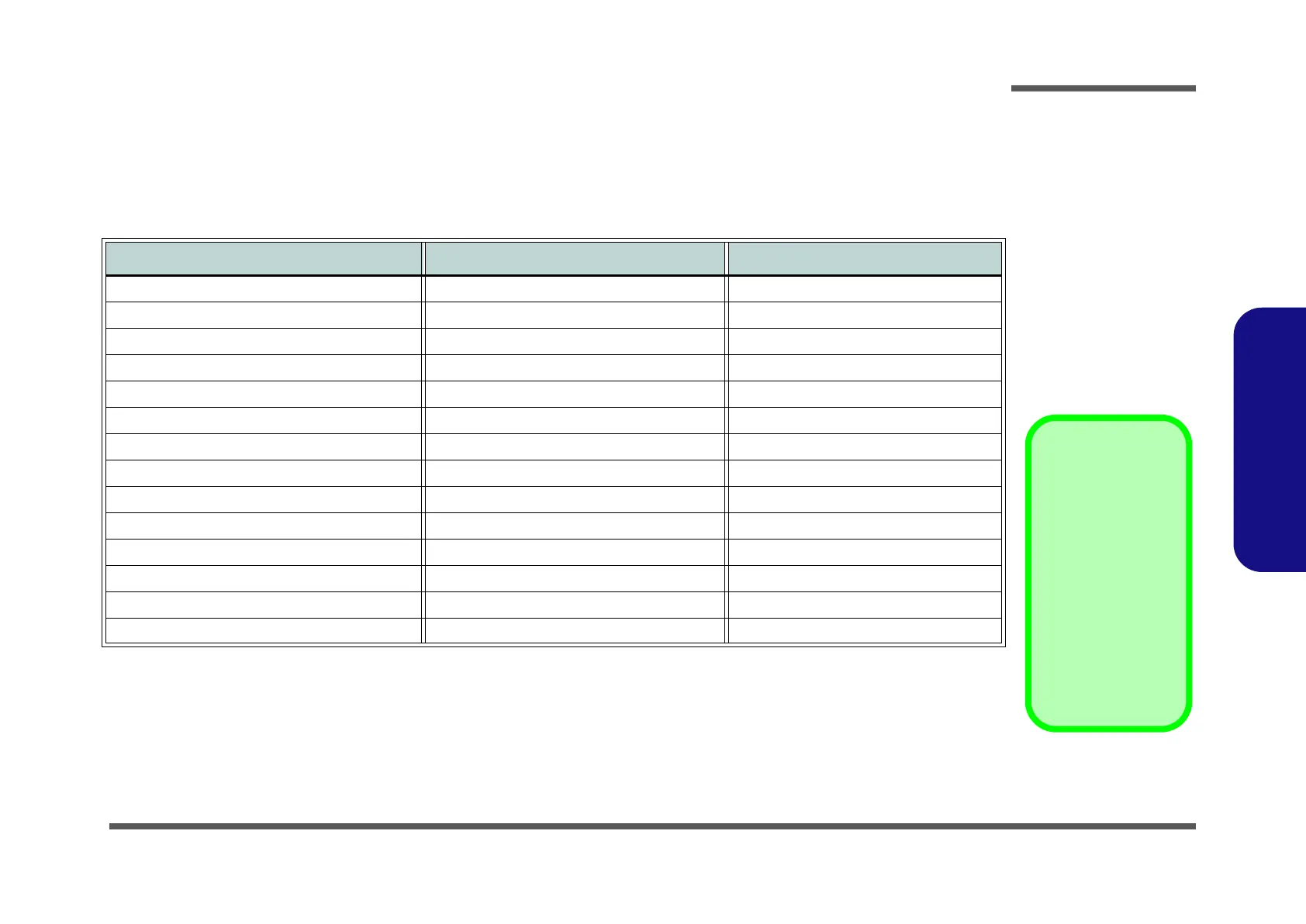
This appendix has circuit diagrams of the W241BU/W241BUQ/W240BU/W245BUQ/W248BUQ/W249BUQ note-
book’s PCB’s. The following table indicates where to find the appropriate schematic diagram.
Diagram - Page Diagram - Page Diagram - Page
System Block Diagram - Page B - 2 HUDSON PCIE/ PCI/ CLOCK/ FCH - Page B - 16 USB/ FAN/ TP/ MULTI CON - Page B - 30
ONTARIO MEM & PCIE I/F, AP - Page B - 3 HUDSON GPIO/ USB/ STRAP - Page B - 17 5VS/ 3.3VS/ 1.8VS/ 1.5VS/ 1.1VS - Page B - 31
ONTATIO DISPLAY/ CLK/ MISC - Page B - 4 HUDSON SATA/ DEBUG IO/ SPI - Page B - 18 POWER VDD3/ VDD5 - Page B - 32
ONTARIO POWER & DECOUPLING - Page B - 5 HUDSON POWER DECOUPLING - Page B - 19 Power 1.5V/ 0.75 - Page B - 33
INAGUA DDR3 SO-DIMMS A - Page B - 6 POWERGOOD/ TPM - Page B - 20 Power 1.1V/ 1VS - Page B - 34
INAGUA DDR3 SO-DIMMS B - Page B - 7 LVDS, INVERTER - Page B - 21 Power 1.8VS - Page B - 35
Robson S3 PCIE/ LVDS 1/6 - Page B - 8 HDMI/ CRT - Page B - 22 APU CORE/ NB CORE - Page B - 36
Robson S3 MAIN 2/6 - Page B - 9 CCD/ 3G - Page B - 23 VGA POWER - Page B - 37
Robson S3 MEM Interface 3/6 - Page B - 10 Card Reader/ LAN JMC261C - Page B - 24 CHARGER/ DC IN - Page B - 38
Robson S3 Straps 4/6 - Page B - 11 MINI PCIE/ SATA HDD/ ODD - Page B - 25 Click Board - Page B - 39
Robson S3 Power 5/6 - Page B - 12 AUDIO CODEC ALC261C - Page B - 26 Audio Board/ USB - Page B - 40
Robson S3 Power 6/6 - Page B - 13 USB 3.0 VL800 - Page B - 27 Power Switch & LID Board - Page B - 41
Robson DDR3 MEM CH-A - Page B - 14 KBC- ITE IT8518 - Page B - 28 EXTERNAL ODD Board - Page B - 42
Robson DDR3 MEM CH-B - Page B - 15 LED/ MDC/ BT - Page B - 29
Table B - 1
Schematic
Diagrams
Version Note
The schematic dia-
grams in this chapter
are based upon ver-
sion 6-7P-W2405-
003. If your main-
board (or other
boards) are a later
version, please
check with the Serv-
ice Center for updat-
ed diagrams (if
required).