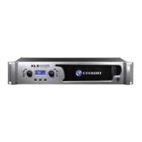
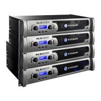
AMPLIFIER SECTION THEORY OF OPERATION
Amplifier Block Diagram: One channel shown w/ common Ruby
Since the 2 channels are the same we will discuss just channel one and know that the
same applies to channel two.
Balanced to unbalanced input stage.
The channel one balanced audio enters the amplifier at one of the back panel connectors
J101, J102 or J3. The signal is then routed to the APM (Audio Processing Module)
through J700B pins 3 and 4. The function of the APM is covered elsewhere in this
document. The signal returns from the APM on J700B pins 6 and 7. It is converted from
balanced to un-balanced at U101B where it is filtered before being combined with the
feedback signal at the junction of R108 and R115. This combined signal connects to the
error amplifier opamp inside the Ruby IC ( U1 ) at pin 61. We will go into detail of the
Ruby IC a little later but for now let’s look at the feedback circuitry.
Feedback Circuits.
The feedback circuit is comprised of two distinct feedback paths, the High Frequency
feedback and the Low Frequency feedback.
The Low frequency feedback comes directly from the output signal at the output relay
which maximizes the damping factor. The Low Frequency feedback is fed into U101D,
pin 13, through the resistors R132 and R133. This circuit attenuates the output signal to a
level acceptable to U101C, provides the 2V DC offset required by the Ruby error
amplifier, filters out the higher frequency switching content and provides the low
frequency/DC feedback to be summed with the High Frequency Feedback.