- 5 -
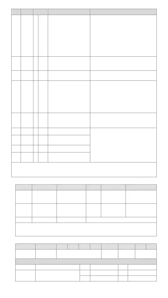
CR# Add. Attrib. Register name Explanation
H’5678: All setting values are written into
the internal flash memory.
After H’5678 is written into the register, all
setting values will be stored in the flash
memory. After the values are stored, the
value in CR#41 becomes H’FFFF. If the
value written into the register is not
H’5678, the value will automatically return
to H0. For example, if K1 is written into
the register, K1 will return to K0.
#42 H102A X R/W
Restoring DVP01LC-SL
to its factory settings
After H’1A2B is written to CR#42,
DVP01LC-SL will be restored to its
factory settings.
#43 H102B X R/W
Setting the percentage of
signals filtered for CH1
Default: K2 Range: K1 to K9 (Unit: 10%)
#50 H1032 X R Status code
b0 (H’0001): The weight gotten from CH1
is zero. (No load)
b2 (H’0004): The weight gotten from CH1
exceeds the maximum weight. (Overload)
b4 (H’0010): The measured value gotten
from CH1 is stable.
b6 ~ b15: Reserved
#51 H1033 X R Error code
All error statuses are stored in the
register. See “Error Code Table” below.
Default: H’0000
#52 H1034 O R/W RS-232 station address
The default in CR#52 and CR#54 is K1.
Range: K1~K255
The default in CR#53 and CR#55 is
H’0000; Range: ASCII, 9600, 7, E, 1.
See “Communication Format Table”
below.
#53 H1035 O R/W
RS-232 communication
format
#54 H1036 O R/W RS-485 station address
#55 H1037 O R/W
RS-485 communication
format
Symbols: O indicates that the register is a latched register. X indicates that the register is not a
latched register.
R indicates that the data can be read. W indicates that the data can be written.
Error Code Table for CR#51:
bit Value Error bit Value Error
b0 K1 (H’0001)
The power
supply is
abnormal.
b1 K2 (H’0002)
The hardware
breaks down.
b2 K4 (H’0004)
The conversion
gotten from CH1
is incorrect.
b3 K8 (H’0008)
The voltage of
SEN in CH1 is
incorrect.
b6 ~ b15 K64 (H’0040) Reserved
Note: Every error status depends on its corresponding bit. There may be more than two
error statuses occurring at the same time. 0 indicates that there is no error. 1
indicates that an error occurs.
Communication Format Table for CR#53, CR#55:
bit15 bit14~bit8 bit7 bit6 bit5 bit4 bit3 bit2 bit1 bit0
ASCII/RTU Reserved Serial transmission speed
Data
length
Stop bit Parity bit
Description
bit15 ASCII/RTU
0 ASCII 1 RTU
bit7~bit4 Serial transmission speed
0 9,600 bps 1 19,200 bps
2 38,400 bps 3 57,600 bps
 Loading...