- 3 -
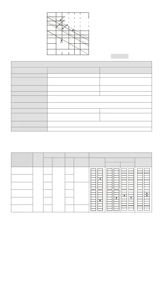
#2: Life curves
Contact
Current(A)
0.5
0.1
0.2
50
0.3 0.7 1 2
200
300
500
100
1000
2000
3000
O
p
e
r
a
t
i
o
n
(
X
1
0
)
3
120VAC Resistive
30VDC Inductive(t=7ms)
240VAC Inductive(cos 0.4)
ψ
=
120VAC Inductive(cos =0.4)
ψ
30VDC
Inductive
(t=40ms)
[ Figure 3 ]
Specifications for analog inputs (Only applicable to DVP24SV11T2)
Voltage input Current input
Analog input range 0 ~ 10V 0 ~ 20mA
Digital conversion
range
0 ~ 4,000 0 ~ 2,000
Resolution 12-bit (2.5mV) 11-bit (10uA)
Input impedance > 1MΩ 250Ω
Overall accuracy
1% of full scale within the range of PLC operation temperature
Response time 2ms (It can be set by means of D1118.)
#1
Absolute input range ±15V ±32mA
Digital data format
16-bit 2’s complement (12
significant bits)
16-bit 2’s complement (11
significant bits)
Average function Provided (It can be set by means of D1062)
#2
Isolation method No isolation between digital circuits and analog circuits
#1: If the scan cycle is longer than 2 milliseconds or greater than the setting value, the scan
cycle is given preference.
#2: If the value in D1062 is 1, the present value is read.
I/O Configuration
Model Power
Input Output I/O configuration
Point Type Point Type Relay
Transistor (NPN)
Transistor
(PNP)
28SV 24SV2
DVP28SV11R
24
VDC
16
DC
(Sink Or
Source)
12
Relay
S/S
X0
X1
X2
X3
X4
X5
X6
X7
S/S
X10
X11
X12
X13
X15
X16
X17
C0
Y0
Y1
Y2
Y3
Y4
Y5
Y6
Y7
Y10
Y11
Y12
Y13
C1
C2
C3X14
S/S
X0
X1
X2
X3
X4
X5
X6
X7
S/S
X10
X11
X12
X13
X15
X16
X17
C0
Y0
Y1
C1
C2
Y4
Y5
Y6
Y7
Y12
Y13
C3
Y2
Y3
C4
Y10
Y11
X14
S/S
X0
X1
X2
X3
X4
X5
X6
X7
X10
X11
V0+
C0
Y0
Y1
C1
C2
Y4
Y5
Y6
Y7
Y12
Y13
C3
Y2
Y3
C4
Y10
Y11
I0+
VI0-
V1+
I1+
VI1-
S/S
X0
X1
X2
X3
X4
X5
X6
X7
S/S
X10
X11
X12
X13
X15
X16
X17
UP0
ZP0
Y0
Y1
Y4
Y5
Y6
Y12
Y13
Y7
Y2
Y3
Y10
Y11
X14
UP1
ZP1
DVP28SV11R2 16 12
DVP28SV11T 16 12
Transistor
(NPN)
DVP28SV11T2 16 12
DVP24SV11T2 10 12
DVP28SV11S2 16 12
Transistor
(PNP)
 Loading...