34
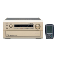
AVR-5803/AVC-A1SR
PCM1804 (IC806, 856, 906, 956)
2
3
4
5
6
7
8
9
10
11
12
13
14
28
27
26
25
24
23
22
21
20
19
18
17
16
15
VREFL
AGNDL
V
COML
V
INL+
V
INL
-
FMT0
FMT1
S/M
OSR0
OSR1
OSR2
BYPAS
DGND
V
DD
VREFR
AGNDR
V
COMR
V
INR+
V
INR
-
AGND
V
CC
OVFL
OVFR
RST
SCKI
LRCK/DSDBCK
BCK/DSDL
DATA/DSDR
TOP VIEW
SN74LV244APW (IC613, 614)
1
2
3
4
5
6
7
8
20
19
18
17
16
15
14
13
1OE
1A1
2Y4
1A2
2Y3
1A3
2Y2
1A4
Vcc
2OE
1Y1
2A4
1Y2
2A3
1Y3
2A2
SCKI
V
IN
L+
V
COM
L
AGNDL
V
REF
L
V
REF
R
AGNDR
V
COM
R
V
IN
R+
V
IN
R
-
OSR0
OSR1
OSR2
S/M
FMT0
FMT1
LRCK/
DSDBCK
BCK/DSDL
DATA/DSDR
OVFL
OVFR
BYPAS
RST
CLK Control
V
IN
L
-
DGND V
DD
AGNDV
CC
Delta-sigma
Modulator (L)
V
REF
L
V
REF
R
Delta-sigma
Modulator (R)
Power Supply
Decimation
Filter (L)
Decimation
Filter (R)
HPF
HPF
Serial
Output
Interface
9
10
12
11
2Y1
GND
1Y4
2A1
1OE
1
1A1
2
1A2
4
1A3
6
1A4
8
18
16
14
12
1Y1
1Y2
1Y3
1Y4
2OE
19
2A1
11
2A2
13
2A3
15
2A4
17
9
7
5
3
2Y1
2Y2
2Y3
2Y4
SN65LVDS179DGK
(IC524)
1
2
3
4
8
7
6
5
V
CC
R
D
GND
A
B
Z
Y
D
3
R
2
5
6
Y
Z
8
7
A
B
Pin Name
Function
PCM1804 Terminal Function
Pin
No.
1VREFL L-channel voltage reference output, requires capacitors for decoupling to AGND.
2 AGNDL Analog ground for VREFL.
3VCOML L-channel analog common mode output.
4VINL+ I L-channel analog input, positive pin.
5VINL− I L-channel analog input, negative pin.
6 FMT0 I Audio data format 0. See TABLE V. *
7 FMT1 I Audio data format 1. See TABLE V. *
8 S/M I Master/slave mode selection. See TABLE IV. *
9 OSR0 I Oversampling ratio 0. See TABLE I. TABLE II. *
10 OSR1 I Oversampling ratio 1. See TABLE I. TABLE II. *
11 OSR2 I Oversampling ratio 2. See TABLE I. TABLE II. *
12 BYPAS I HPF bypass control. HIGH: HPF disable, LOW: HPF enable. ***
13 DGND Digital ground.
14 VDD Digital power supply.
15 DATA/DSDR O
L-channel and R-channel audio data output in PCM mode. R-channel Audio data output in DSD mode.(DSD output, when DSD mode)
16 BCK/DSDL I/O Bit clock input/output in PCM mode. L-channel audio data output in DSD mode. ***
17 LRCK/DSDBCK I/O Sampling clock input/output in PCM and DSD mode. ***
18 SCKI I System clock input; 128fs, 256fs, 384fs, 512fs or 768fs. **
19 RST I Reset, power down input, active LOW. *
20 OVFR O Overflow signal of R-channel in PCM mode. This is available in PCM mode only.
21 OVFL O Overflow signal of L-channel in PCM mode. This is available in PCM mode only.
22 VCC Analog power supply.
23 AGND Analog ground.
24 VINR− I R-channel analog input, negative pin.
25 VINR+ I R-channel analog input, positive pin.
26 VCOMR R-channel analog common mode output.
27 AGNDR Analog ground for VREFR.
28 V
REFR R-channel voltage reference output, requires capacitors for decoupling to AGND.
I/O
* Schmitt trigger input with internal pull-down (51kW typically), 5V tolerant.
** Schmitt trigger input, 5V tolerant.
*** Schmitt trigger input.