ADV7623 Hardware Manual
Rev. 0 – March 2010 18 Confidential NDA required
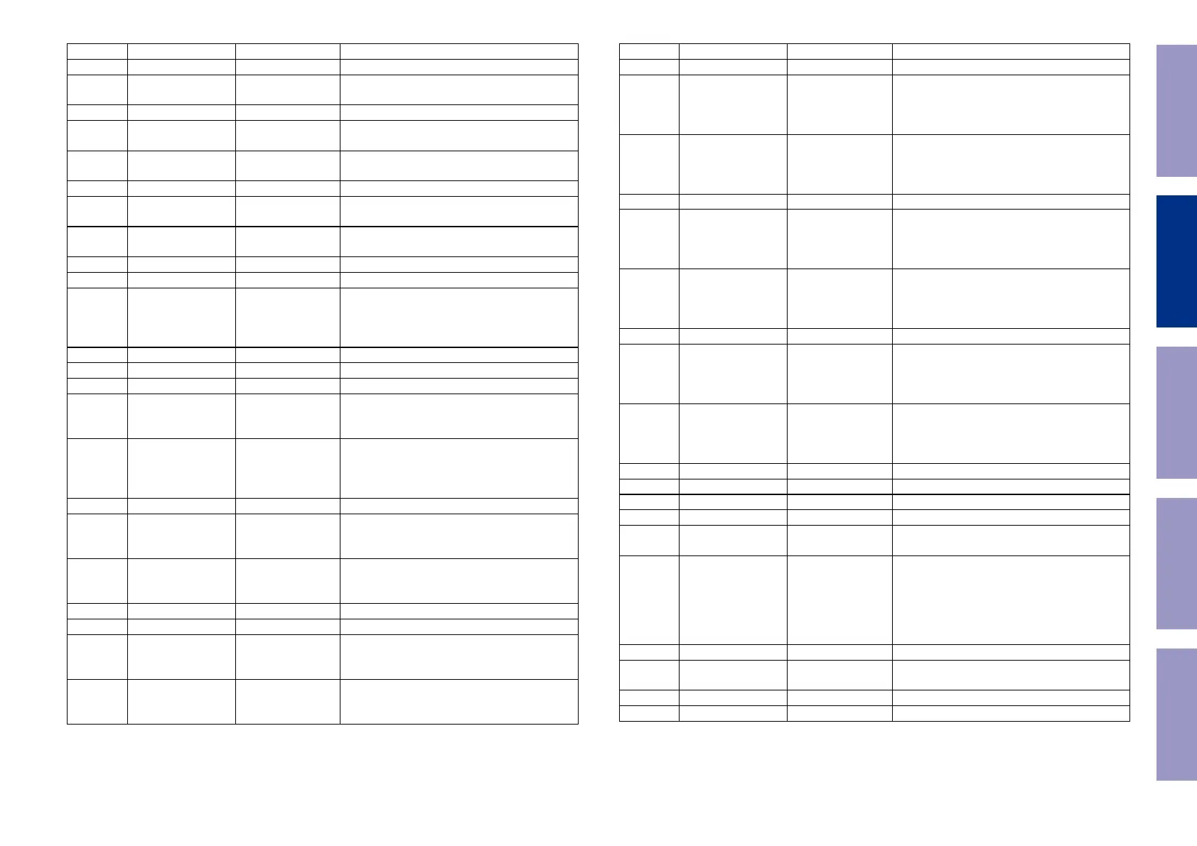
Location Mnemonic Type Description
D in the HDMI interface.
27 RXD_0+ HDMI Input Digital input channel 0 True of port D in
the HDMI interface.
28 CGND Ground TVDD and CVDD Ground
29 RXD_1- HDMI Input Digital input channel 1 complement of port
D in the HDMI interface.
30 RXD_1+ HDMI Input Digital input channel 1 true of port D in the
HDMI interface.
31 TVDD Power Receiver terminator supply voltage (3.3 V)
32 RXD_2- HDMI Input Digital input channel 2 complement of port
D in the HDMI interface.
33 RXD_2+ HDMI Input Digital input channel 2 true of port D in the
HDMI interface.
34 CVDD Power Receiver comparator supply voltage (1.8V)
35 CGND Ground TVDD and CVDD Ground
36 TXPVDD Power 1.8 V Power Supply for Digital and I/O
Power Supply. These pins supply power to
the digital logic and I/Os. They should be
filtered and as quiet as possible.
37 TXPLVDD Power 1.8 V Power Supply.
38 TXGND Ground TXPVDD Ground
39 TXPGND Ground TXPLVDD Ground
40 EXT_SWING Analog Input Sets Internal Reference Currents. Place 887
Ω resistor (1% tolerance) between this pin
and ground.
41 HPD_ARC- Analog Input Hot Plug Detect Signal. This indicates to
the interface whether the receiver is
connected. Supports 1.8 V to 5.0V CMOS
logic levels.
42 ARC+ Analog Input Audio return channel input
43 TXDDC_SDA Digital I/O Serial Port Data I/O to Receiver. This pin
serves as the master to the DDC bus.
Supports a 5 V CMOS logic level.
44 TXDDC_SCL Digital Input Serial Port Data Clock to Receiver. This pin
serves as the master clock for the DDC bus.
Supports a 5 V CMOS logic level.
45 TXAVDD Power 1.8V power supply for TMDS outputs
46 TXGND Ground TXAVDD Ground
47 TXC- HDMI Output Differential Clock Output. Differential
clock output at the TMDS clock rate;
supports TMDS logic level.
48 TXC+ HDMI Output Differential Clock Output. Differential
clock output at the TMDS clock rate;
supports TMDS logic level.
ADV7623 Hardware Manual
Rev. 0 – March 2010 19 Confidential NDA required
Location Mnemonic Type Description
49 TXGND Ground TXAVDD Ground
50 TX0- HDMI Output Differential Output Channel 0
Complement. Differential output of the red
data at 10× the pixel clock rate; supports
TMDS logic level.
51 TX0+ HDMI Output Differential Output Channel 0 True.
Differential output of the red data at 10×
the pixel clock rate; supports TMDS logic
level.
52 TXGND Ground TXAVDD Ground
53 TX1- HDMI Output Differential Output Channel 1
Complement. Differential output of the red
data at 10× the pixel clock rate; supports
TMDS logic level.
54 TX1+ HDMI Output Differential Output Channel 1 True.
Differential output of the red data at 10×
the pixel clock rate; supports TMDS logic
level.
55 TXAVDD Power 1.8V power supply for TMDS outputs
56 TX2- HDMI Output Differential Output Channel 2
Complement. Differential output of the red
data at 10× the pixel clock rate; supports
TMDS logic level.
57 TX2+ HDMI Output Differential Output Channel 2 True.
Differential output of the red data at 10×
the pixel clock rate; supports TMDS logic
level.
58 TXGND Ground TXAVDD Ground
59 CEC Digital I/O Consumer electronic control channel.
60 DGND Ground Ground for DVDD
61 DVDD Power Digital supply voltage (1.8 V)
62 ALSB Digital Input This pin is used to set I2C address of the Rx
IO and the Tx Main Map.
63 CSB Digital Input Chip Select pin. This pin must be set low or
left floating for the chip to process I2C
messages that are destined to the
ADV7623. The ADV7623 ignores I2C
messages which he receives if this pin is
high.
64 EP_SCK Digital Output SPI clock interface for the EDID/OSD
65 EP_CS Digital Output SPI chip selected interface for the
EDID/OSD
66 EP_MOSI Digital Output SPI master out/slave in for the EDID/OSD
67 EP_MISO Digital Input SPI master in/slave out for the EDID/OSD
Before Servicing
This Unit
Electrical Mechanical Repair Information Updating
37
 Loading...