MC74HC4094ADR2G (DIGITAL_MCU : IC752, IC753)
Logic Diagram
MC74HC4094A
http://onsemi.com
2
13
14
15
16
9
10
11
125
4
3
2
1
8
7
6
QP
6
QP
5
QP
4
OE
V
CC
QS
1
QS
2
QP
7
QP
0
CP
D
STR
GND
QP
3
QP
2
QP
1
Figure 1. Pin Assignment
Figure 2. Logic Symbol Figure 3. IEC Logic Symbol
CP STR
31
2
9
10
4
5
6
7
14
13
12
11
15
DD
OE
QS1
QS2
QP0
QP1
QP2
QP3
QP4
QP5
QP6
QP7
3
1
2
9
10
4
5
6
7
14
13
12
11
15
1 D 2 D 3
C1/
SRG8
C2
EN3
Figure 4. Functional Diagram
8 – Stage Shift Register
8 – Bit Storage Register
3 – Stage Outputs
QP0 QP1 QP2 QP3 QP4 QP5 QP6 QP7
4 5 6 7 14 13 12 11
2
3
1
15
10
9
D
CP
STR
OE
QS2
QS1
MC74HC4094A
http://onsemi.com
3
Figure 5. Logic Diagram
QP1 QP2 QP3 QP4 QP5 QP6
D
CP
STR
OE
STAGES 1 TO 6STAGE 0 STAGE 7
QP
7QP0
QS1
QS2
D
CP
Q
FF0
D
CP
Q
latch
D
CP
Q
FF7
D
CP
Q
latch
D
CP
Q
latch
CP
D
Q
SN74LVC244APWR (DIGITAL_OSD : IC734)
(DIGITAL_PLD : IC772)
(DIGITAL_DSP : IC783)
(DIGITAL_LEGO : IC812)
(DIGITAL_HDMI_TX : IC722)
Block diagram
FEATURES
DESCRIPTION/ORDERING INFORMATION
1
2
3
4
5
6
7
8
9
10
20
19
18
17
16
15
14
13
12
11
1OE
1A1
2Y4
1A2
2Y3
1A3
2Y2
1A4
2Y1
GND
V
CC
2OE
1Y1
2A4
1Y2
2A3
1Y3
2A2
1Y4
2A1
DB, DGV, DW, N, NS, OR PW PACKAGE
(TOP VIEW)
RGY PACKAGE
(TOP VIEW)
1 20
10 11
2
3
4
5
6
7
8
9
19
18
17
16
15
14
13
12
2OE
1Y1
2A4
1Y2
2A3
1Y3
2A2
1Y4
1A1
2Y4
1A2
2Y3
1A3
2Y2
1A4
2Y1
1OE
2A1
V
GND
CC
SN74LVC244A
OCTAL BUFFER/DRIVER
WITH 3-STATE OUTPUTS
SCAS414X–NOVEMBER 1992 –REVISED MARCH 2005
• Operates From 1.65 V to 3.6 V
• Inputs Accept Voltages to 5.5 V
• Specified From –40°C to 85°C and –40°C to
125°C
• Max t
pd
of 5.9 ns at 3.3 V
• Typical V
OLP
(Output Ground Bounce) < 0.8 V
at V
CC
= 3.3 V, T
A
= 25°C
• Typical V
OHV
(Output V
OH
Undershoot) > 2 V
at V
CC
= 3.3 V, T
A
= 25°C
• Supports Mixed-Mode Signal Operation on All
Ports (5-V Input/Output Voltage With
3.3-V V
CC
)
• I
off
Supports Partial-Power-Down Mode
Operation
• Latch-Up Performance Exceeds 250 mA Per
JESD 17
• ESD Protection Exceeds JESD 22
– 2000-V Human-Body Model (A114-A)
– 200-V Machine Model (A115-A)
– 1000-V Charged-Device Model (C101)
This octal buffer/line driver is operational at 1.5-V to
3.6-V V
CC
, but is designed specifically for 1.65-V to
3.6-V V
CC
operation.
ORDERING INFORMATION
T
A
PACKAGE
(1)
ORDERABLE PART NUMBER TOP-SIDE MARKING
QFN – RGY Reel of 1000 SN74LVC244ARGYR LC244A
–40°C to 85°C VFBGA – GQN SN74LVC244AGQNR
Reel of 1000 LC244A
VFBGA – ZQN (Pb-Free) SN74LVC244AZQNR
PDIP – N Tube of 20 SN74LVC244AN SN74LVC244AN
Tube of 25 SN74LVC244ADW
SOIC – DW LVC244A
Reel of 2000 SN74LVC244ADWR
SOP – NS Reel of 2000 SN74LVC244ANSR LVC244A
–40°C to 125°C SSOP – DB Reel of 2000 SN74LVC244ADBR LC244A
Tube of 70 SN74LVC244APW
TSSOP – PW Reel of 2000 SN74LVC244APWR LC244A
Reel of 250 SN74LVC244APWT
TVSOP – DGV Reel of 2000 SN74LVC244ADGVR LC244A
(1) Package drawings, standard packing quantities, thermal data, symbolization, and PCB design guidelines are available at
www.ti.com/sc/package.
Please be aware that an important notice concerning availability, standard warranty, and use in critical applications of Texas
Instruments semiconductor products and disclaimers thereto appears at the end of this data sheet.
PRODUCTION DATA information is current as of publication date.
Copyright © 1992–2005, Texas Instruments Incorporated
Products conform to specifications per the terms of the Texas
Instruments standard warranty. Production processing does not
necessarily include testing of all parameters.
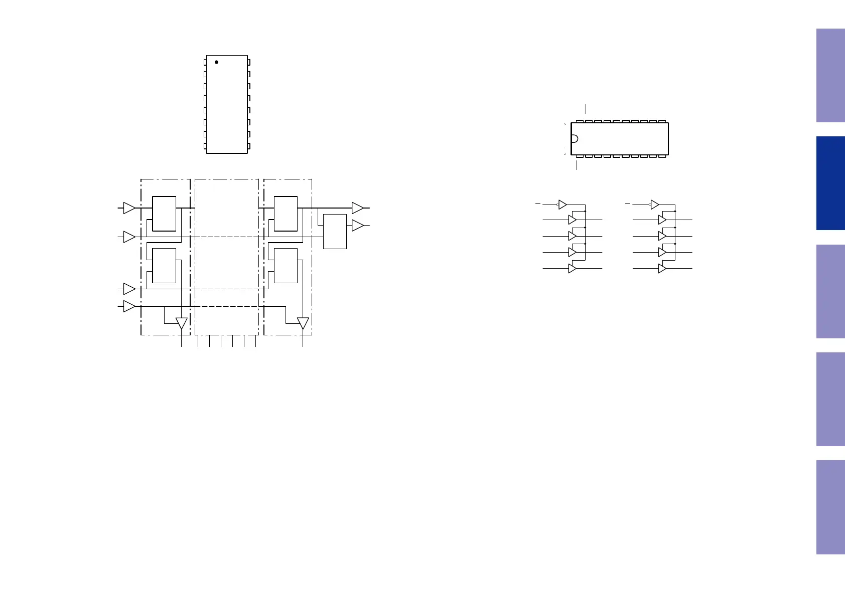
1
2 18
1Y1
1OE
1A1
4 16
1Y2
1A2
6 14
1Y3
1A3
8 12
1Y4
1A4
19
11 9
2OE
2A1
13 7
2A2
15 5
2A3
17 3
2A4
Pin numbers shown are for the DB, DGV, DW, N, NS, PW, and RGY packages.
Absolute Maximum Ratings
(1)
SN74LVC244A
OCTAL BUFFER/DRIVER
WITH 3-STATE OUTPUTS
SCAS414X– NOVEMBER 1992 –REVISED MARCH 2005
LOGIC DIAGRAM (POSITIVE LOGIC)
over operating free-air temperature range (unless otherwise noted)
MIN MAX UNIT
V
CC
Supply voltage range –0.5 6.5 V
V
I
Input voltage range
(2)
–0.5 6.5 V
V
O
Voltage range applied to any output in the high-impedance or power-off state
(2)
–0.5 6.5 V
V
O
Voltage range applied to any output in the high or low state
(2)(3)
–0.5 V
CC
+ 0.5 V
I
IK
Input clamp current V
I
< 0 –50 mA
I
OK
Output clamp current V
O
< 0 –50 mA
I
O
Continuous output current ±50 mA
Continuous current through V
CC
or GND ±100 mA
DB package
(4)
70
DGV package
(4)
92
DW package
(4)
58
GQN/ZQN package
(4)
78
θ
JA
Package thermal impedance °C/W
N package
(4)
69
NS package
(4)
60
PW package
(4)
83
RGY package
(5)
37
T
stg
Storage temperature range –65 150 °C
P
tot
Power dissipation T
A
= –40°C to 125°C
(6)(7)
500 mW
(1) Stresses beyond those listed under "absolute maximum ratings" may cause permanent damage to the device. These are stress ratings
only, and functional operation of the device at these or any other conditions beyond those indicated under "recommended operating
conditions" is not implied. Exposure to absolute-maximum-rated conditions for extended periods may affect device reliability.
(2) The input and output negative-voltage ratings may be exceeded if the input and output current ratings are observed.
(3) The value of V
CC
is provided in the recommended operating conditions table.
(4) The package thermal impedance is calculated in accordance with JESD 51-7.
(5) The package thermal impedance is calculated in accordance with JESD 51-5.
(6) For the DW package: above 70°C the value of P
tot
derates linearly with 8 mW/K.
(7) For the DB, DGV, N, NS, and PW packages: above 60°C the value of P
tot
derates linearly with 5.5 mW/K.
3
Before Servicing
This Unit
Electrical Mechanical Repair Information Updating
50
 Loading...