Copyright Digilent, Inc. All rights reserved.
Other product and company names mentioned may be trademarks of their respective owners.
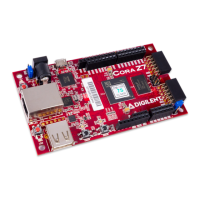
FPGA user I/O, USB Controller, Flash Memory, Pmod
Connector, LEDs, Buttons
Table 1.1. Power rail characteristics.
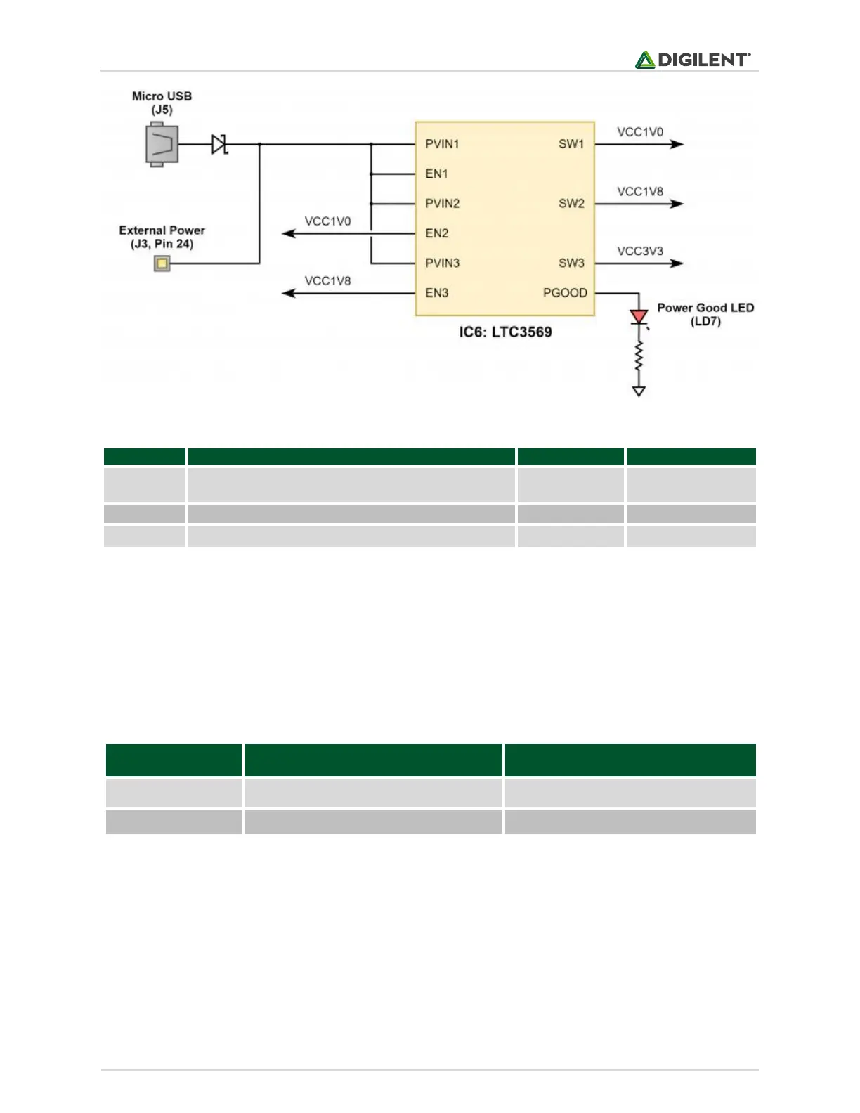
1.1 Power Input Options
It is possible to power the PLTW S7 from either USB or from an external power supply attached to pins 24 and 25
of the DIP headers, labeled “VU” and “GND”, respectively. The required characteristics of a power source attached
to either of these two options is outlined in Table 1.1.1.
When the PLTW S7 is powered by the USB connector, the voltage from the USB device is driven onto the VU pin.
This makes it possible to power an external circuit from the USB host in addition to the PLTW S7. The VU pin is
driven via a schottky diode, so a small voltage drop will occur, but it should be assumed that the voltage present
on VU will be close to 5V.
Warning: When a USB host is attached to the micro USB connector, the VU pin on the DIP headers (pin 24) is
driven to the voltage being provided by the USB host (typically 4.5V-5.5V). To avoid risk of damage, any power
source attached to the VU pin must be disconnected before a USB host is attached. Not taking this precaution
can be particularly dangerous if the power source is a battery.