29
Signal description (QSPI communication)
Below shows description of I/O signal from target side during QSPI communication
(”I/O” means input and output direction from view of probe side.)
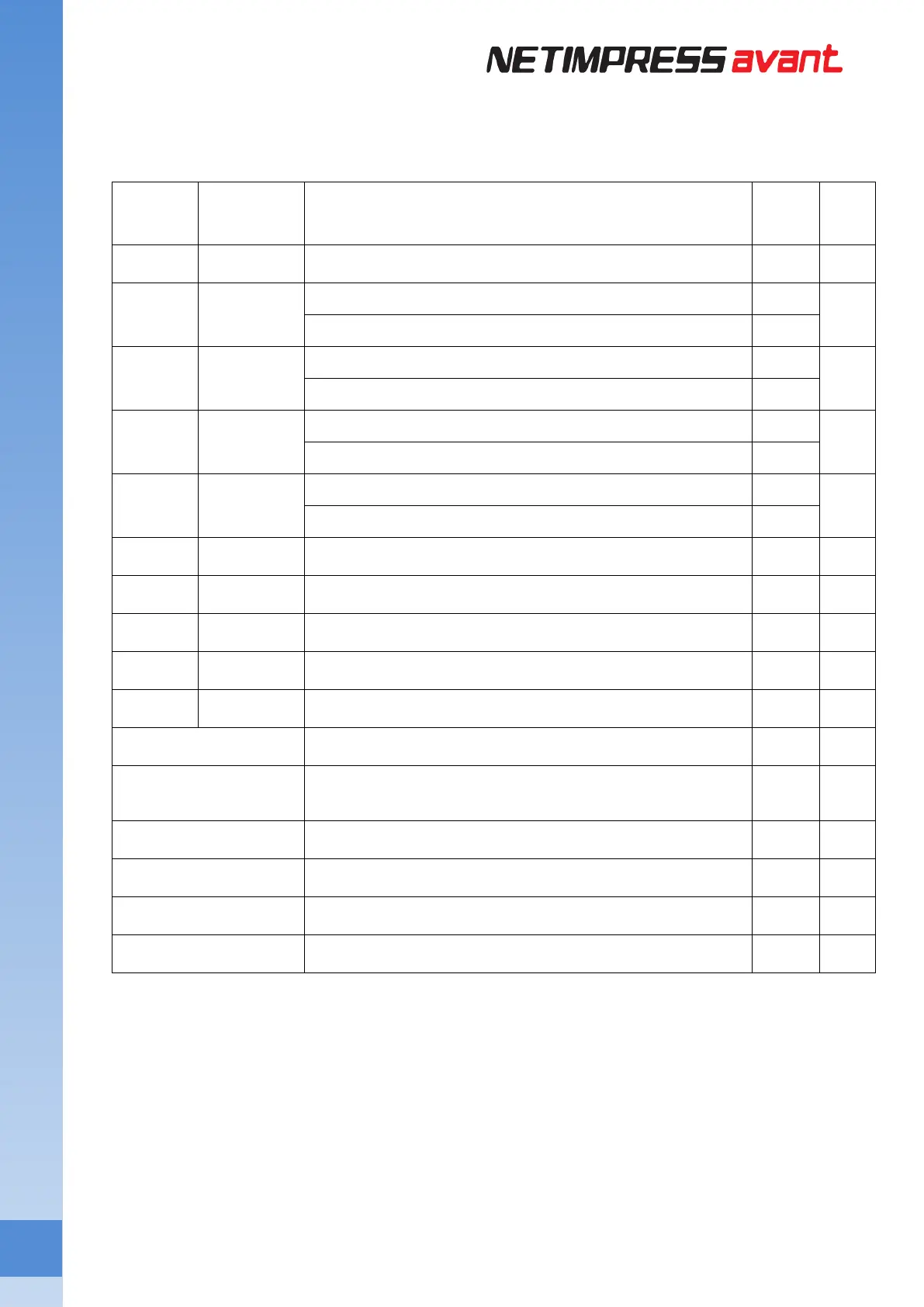
Signal
Name
QSPI
Mode
Meaning I/O Type
IO1 SCK SCK output of SPI O A
IO2 SO/IO0
Transmitted data output of SPI O
A
Input / output in dual or quad modes I/O
IO3 SI/IO1
Received data input of SPI I
A
Input / output in dual or quad modes I/O
IO4 WP#/IO2
WP output of negative logic SPI O
A
Input / output in dual or quad modes I/O
IO5 HOLD#/IO3
HOLD output of negative logic SPI O
A
Input / output in dual or quad modes I/O
IO6 CS# chip select output of negative logic O A
IO7 TAUX3 I/O terminal (definition varies according to definition program) I/O A
IO8 TAUX4 I/O terminal (definition varies according to definition program) I/O B
IO9 TMODE I/O terminal (definition varies according to definition program) I/O B
IO10 /TICS I/O terminal (definition varies according to definition program) I/O B
VCC
5V output (MAX 100mA) O C
/TRES
Re-set output of negative logic (open collector output)
(*1)
O D
WDT Watchdog timer output (open collector output) (*1) O D
TVccd User power input (driver power for I/F) I E
PROBE SELECT Terminal selection signal of target probe I F
GND GND - -
*1 /TRES, WDT are open collector signal with 1MΩ pull down.
Please note that no voltage output to target side.