* All bytes of the main memory are erased, blank checked and programmed with the
randomly generated data used as a code data. Whole MAIN memory content is
verified (check sum) and also read whole data and verified byte by byte.
* One sector (location 0xFC00 to 0xFDFF) is erased and blank checked. Also contents
of the two closer sectors are verified if there are not erased. Small block of data are
saved and verified in the mentioned sector.
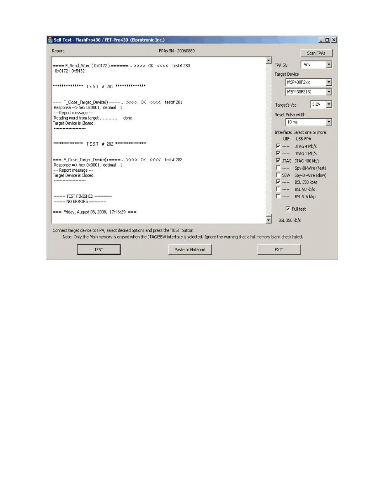
* Word write/read to TACCR0 (0x172) register.
* Byte/Word manipulation are used in the part of the RAM.
2. BSL interface is used (not supported in the MSP-FET430UIF):
* Due to unknown access password, the whole Flash memory - MAIN and INFO are
erased. In the F2xx microcontrollers the DCO calibration data will be erased. There
is no way to save the DCO data if the BSL password is unknown. The DCO data can
Figure 2.1
18