EN
PNP
A
ss
emb
l
y
instructions
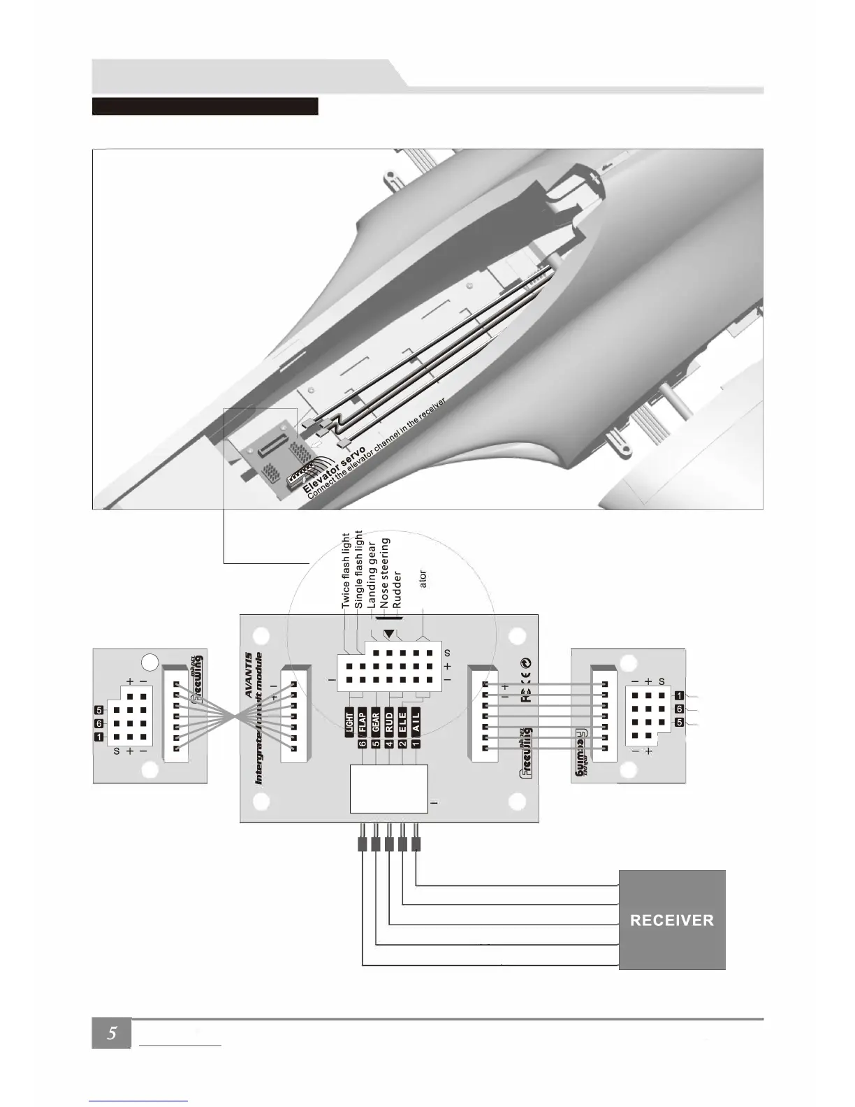
Control board connection diagram
R
q
0
+
0
0
�m
>
�
w
0
• • • • •
s
• • • • •
+
• • • • •
0
T Receiver
0
0
AVANTI S