FULL-WAVE
RECTIFIER
EXPERIENCE
DISCUSSION
The
process
of changing alternating current
(AC)
to direct
current
(DC)
is
called rectification.
A full-wave rectifier uses
both halves of the AC cycle in the rectification
process. That
is, it
produces
one
DC
voltage
pulse
for
each
one-half cycle
of
AC,
as
illustrated in Fig. H.
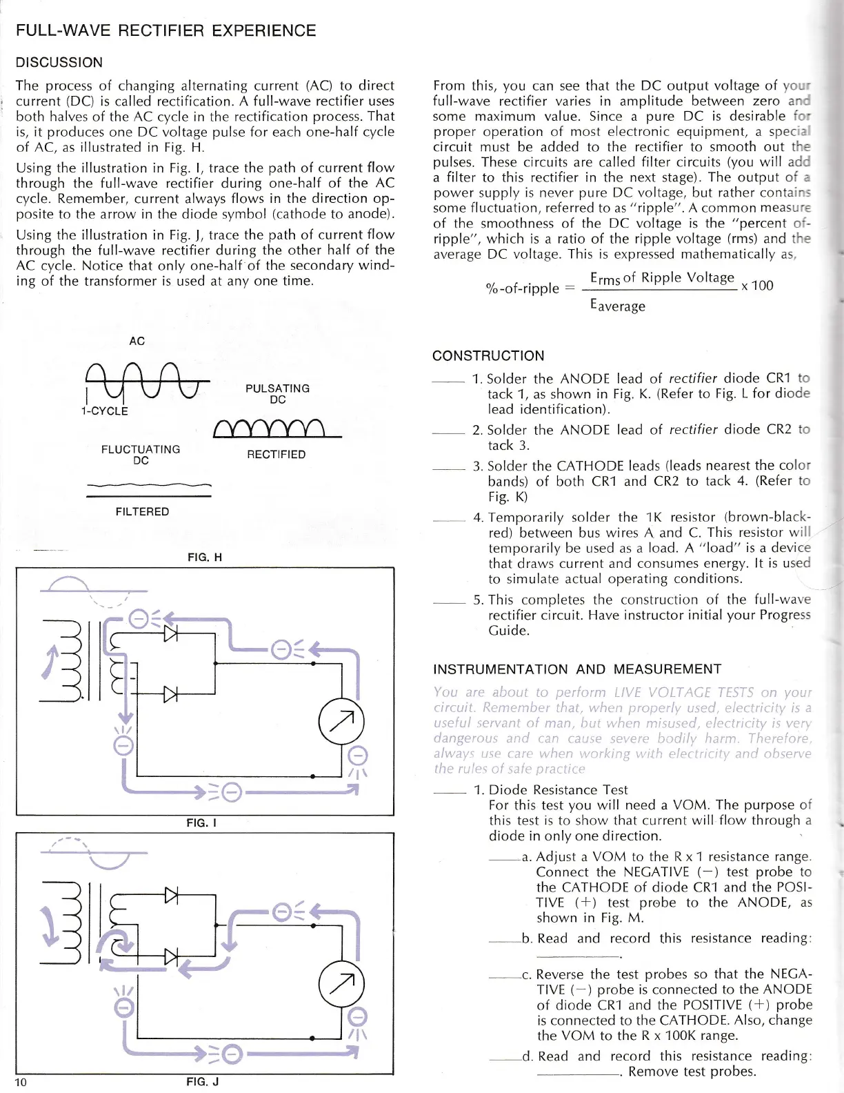
Using the
illustration in
Fig. l, trace the
path
of
current flow
through the full-wave rectifier during one-half
of the AC
cycle. Remember,
current always
flows in the direction op-
posite
to the arrow in the diode symbol
(cathode
to
anode)
.
Using the illustration in Fig.
l,
trace the
path
of
current
flow
through
the full-wave
rectifier
during
the other
half o{ the
AC
cycle. Notice that only one-half of
the secondary
wind-
ing
of the transformer
is
used at any
one time.
From
this,
you
can see that the
DC
output
voltage of
r', .'
full-wave
rectifier varies
in
amplitude between
zero ?'
some
maximum
value. Since a
pure DC is desirab!e
'
'
proper
operation of most electronic equipment, a spe.
circuit must be added to the rectifier to smooth out
t-.
pulses.
These circuits are called
filter
circuits
(you
will a,:
-
a
filter
to this rectifier
in
the next stage)
. The
output
o:.
power
supplv
is never
pure
DC voltage, but rather conta'-.
some
fluctuation, referred
to as
"ripple".
A common
measL.
-.
of the smoothness
of the DC voltage
is
the
"percent.'-
ripple", w.hich is a ratio
of the
ripple voltage
(rms)
and i:-
average DC
voltage. This is
expressed
mathematicall',, 25
%-of-ripple
_
Ermsof Ripple Voltage
*
100
E
average
CONSTRUCTION
-
1.
Solder
the ANODE lead of
rectifier diode
CR1
i:
tack 1, as shown
in Fig. K.
(Refer
to
Fig. L for dioc=
lead identification).
2. Solder the
ANODE lead of
rectifier diode CR2
:
tack 3.
-
-
3. Solder the CATHODE
leads
(leads
nearest
the colc:
bands) of both CR'l
and CR2 to
tack 4.
(Refer
tr,
Fig. K)
-
4. Temporarily solder the
1K resistor
(brown-black-
red) between bus
wires A and C.
This resistor
lr'r
temporarily be used as a
load. A "load"
is
a devict
that draws
current and consumes
energy. lt
is
usec,
to simulate actual
operating conditions.
5. This completes the
construction of the
full-wate
rectifier
circuit. Have
instructor initial
your
Progress
Cuide.
INSTRUMENTATION AND MEASUREMENT
-
-
1. Diode Resistance Test
For this test
you
will need
a
VOM.
The
purpose
c'
this test
is
to show,that current
will flow through
a
diode
in
only
one direction.
a. Adjust a VOM to the R x
1 resistance range.
Connect the NECATIVE
(-)
test
probe
to
the CATHODE of diode CR1
and the
POSI-
TIVE
(+)
test
probe
to the
ANODE, as
shown
in
Fig. M.
b. Read and
record
this
resistance
reading:
-
c.
Reverse the test
probes
so that the NECA-
TIVE
(
)
probe
is connected to the
ANODE
of
diode
CR1 and the
POSITIVE
(l)
probe
is connected to the CATHODE.
Also, change
the
VOM
to the
R x 100K range.
M\N.,
PULSATNG
1-CYCLE
FLUCTUATING
DC
nrrnn^
RECTIFIED
FILTERED
=l
jli
FIG.
d.
Read and record this
Remove
resistance reading
test
probes.
?
E
10
FIG. J
\-/
o<
lt
FIG. H
;o