Service Manual
Model No.:
- 11 -
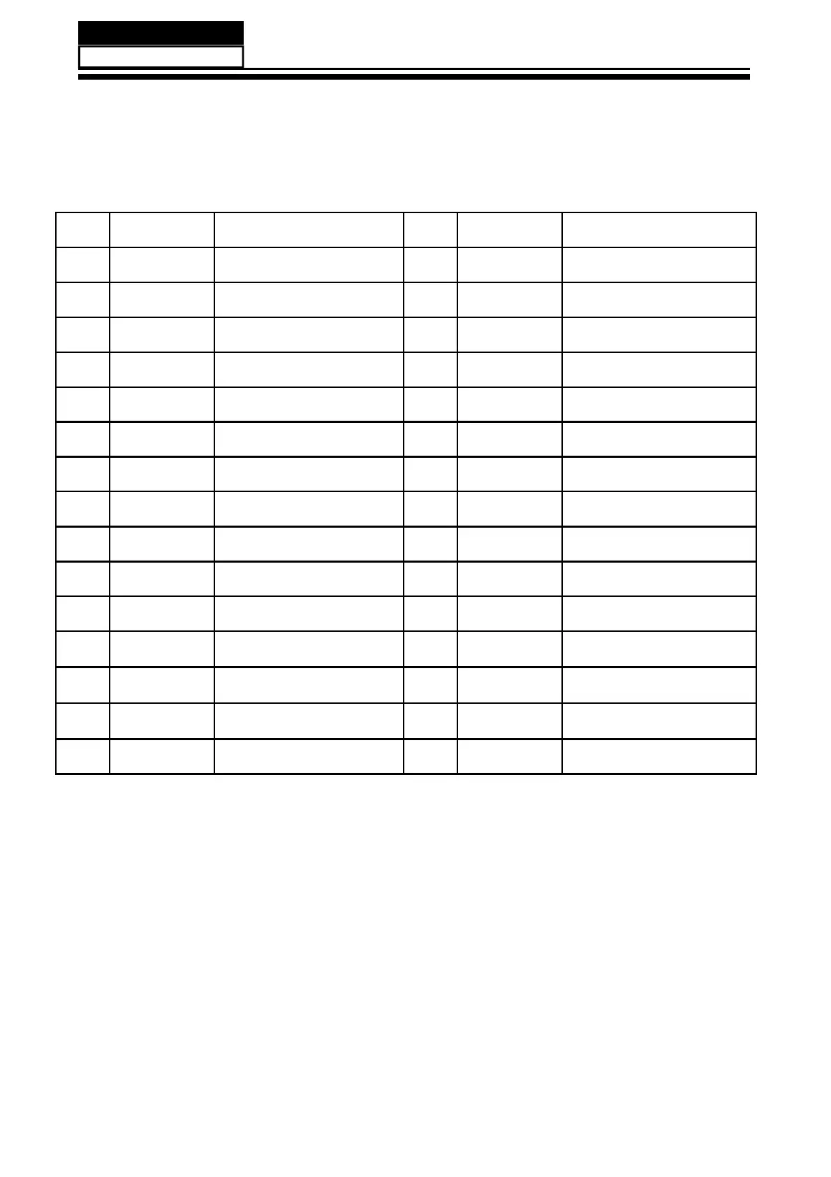
3-4-1.Connector de finition
Pin S
mbol Descri
tion Pin S
mbol Descri
tion
1
12V DC
ower su
l
16
R1B_P LVDS Si
nal +
2
12V DC
ower su
l
17
GND Ground
3
12V DC
ower su
l
18
R1C_N LVDS Si
nal -
4
12V DC
ower su
l
19
R1C_P LVDS Si
nal +
5
GND Ground
20
GND Ground
6
GND Ground
21
R1CLK_N LVDS Clock -
7
GND Ground
22
R1CLK_P LVDS Clock +
8
GND Ground
23
GND Ground
9
LVDS SEL LVDS O
tion
24
R1D_N LVDS Si
nal -
10
NC NOTE1
25
R1D_P LVDS Si
nal +
11
GND Ground
26
GND Ground
12
R1A_N LVDS Signal -
27
TCON_WP
I2C
13
R1A]P LVDS Signal +
28
SCL_I
I2C
14
GND Ground
29
SDA_I
I2C
15
R1B_N LVDS Si
nal -
30
GND Ground
Note (1) No connection: These PINS are used only for the product of SAMSUNG.
(DO NOT CONNECT the input device to these pins.)
Note2) LVDS OPTION : If this P,1LV+,*+9 ମ Normal LVDS format
/2:*1' ମ JEIDA LVDS format

 Loading...