TMP92FD28
2007-01-30
92FD28-6
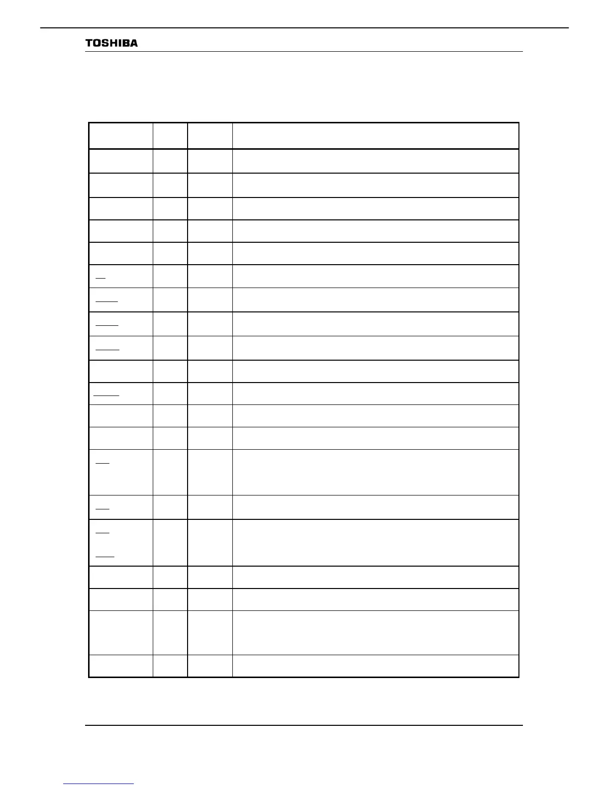
2.2 Pin Names and Functions
The following table shows the names and functions of the input/output pins.
Table 2.2.1 Pin Names and Functions (1/3)
Pin name
Number
of Pin
I/O
Function
P00 to P07
D0 to D7
8 I/O
I/O
Port 0: I/O port Input or output specifiable in units of bits
Data: Data bus 0 to 7
P10 to P17
D8 to D15
8 I/O
I/O
Port 1: I/O port Input or output specifiable in units of bits
Data: Data bus 8 to 15
P40 to P47
A0 to A7
8 I/O
Output
Port 4: I/O port Input or output specifiable in units of bits
Address: Address bus 0 to 7
P50 to P57
A8 to A15
8 I/O
Output
Port 5: I/O port Input or output specifiable in units of bits
Address: Address bus 8 to 15
P60 to P67
A16 to A23
8 I/O
Output
Port 6: I/O port Input or output specifiable in units of bits
Address: Address bus 16 to 23
P70
RD
1 I/O
Output
Port 70: I/O port (Schmitt input, with pull-up register)
Read: Outputs strobe signal for read external memory.
P71
SRWR
1 I/O
Output
Port 71: I/O port (Schmitt input, with pull-up register)
Write enable for SRAM: Strobe signal for wiritng data.
P72
SRLLB
1 I/O
Output
Port 72: I/O port (Schmitt input, with pull-up register)
Data enable for SRAM on pins D0 to D7
P73
SRLUB
1 I/O
Output
Port 73: I/O port (Schmitt input, with pull-up register)
Data enable for SRAM on pins D8 to D15
P74
TA0IN
1 I/O
Input
Port 74: Input port (Schmitt input)
8-bit timer 0 input: Input pin of 8-bit timer TMRA0
P75
USBOC
1 I/O
Input
Port 75: I/O port (Schmitt input)
USBOC Input
P76
USBPON
1 I/O
Output
Port 76: I/O port (Schmitt input)
USBPON Output
P77
X1USB
1 I/O
Input
Port 77: I/O port
48MHz Clock Input for USB Host Controller
P80
0CS
TA1OUT
BOOT
1 Output
Output
Output
Input
Port 80: Output port
Chip select 0: Outputs “Low” when address is within specified address area
8-bit timer 1 Output: Output pin of 8-bit timer TMRA0 or TMRA1
This pin sets single boot mode (only during reset).
P82
2CS
1 Output
Output
Port 82: Output port
Chip select 2: Outputs “Low” when address is within specified address area
P83
3CS
TA5OUT
WAIT
1 I/O
Output
Output
Input
Port 83: I/O port
Chip select 3: Outputs “Low” when address is within specified address area
8-bit timer 5 Output: Output pin of 8-bit timer TMRA4 or TMRA5
Wait: Signal used to request CPU bus wait
PC0
INT0
1 Input
Input
Port C0: Input port (Schmitt input)
Interrupt request pin0 : Interrupt request pin with programmable level/rising/falling edge
PC1
INT1
1 Input
Input
Port C1: Input port (Schmitt input)
Interrupt request pin 1 : Interrupt request pin with programmable level/rising/falling edge
PC2
INT2
TB0IN0
TB1IN0
1 Input
Input
Input
Input
Port C2: Input port (Schmitt input)
Interrupt request pin 2 : Interrupt request pin with programmable level/rising/falling edge
16-bit timer 0 input 0: Input of count/capture trigger in 16-bit timer TMRB0
16-bit timer 1 input 0: Input of count/capture trigger in 16-bit timer TMRB1
PC3
INT3
1 Input
Input
Port C3: Input port (Schmitt input)
Interrupt request pin 3 : Interrupt request pin with programmable level/rising/falling edge
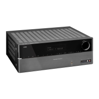
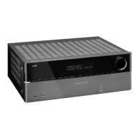
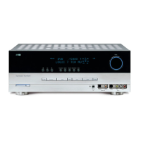
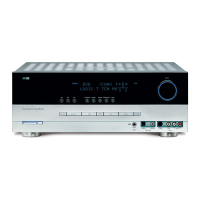
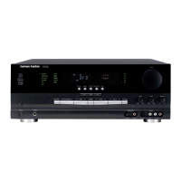
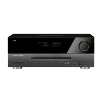
AVR3600 harman/kardon
 Loading...