ADV7342/ADV7343
Rev. 0 | Page 18 of 88
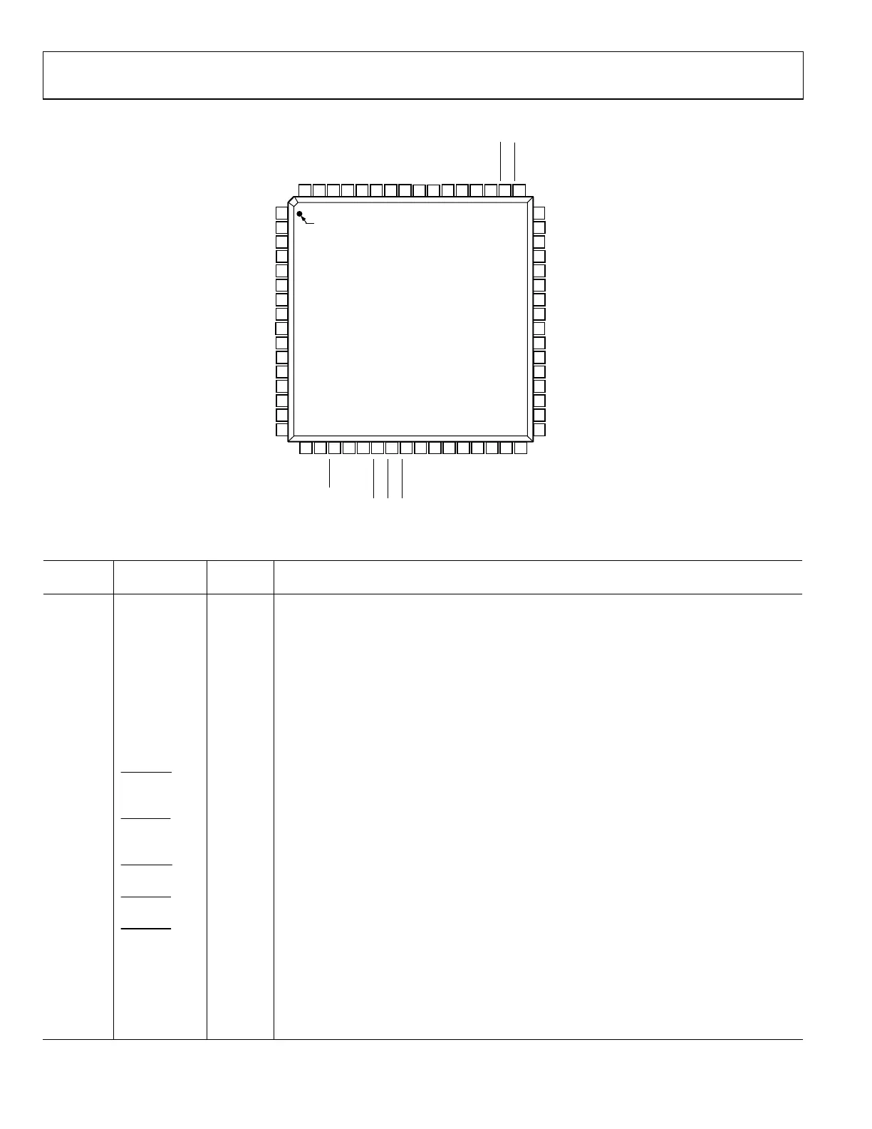
PIN CONFIGURATION AND FUNCTION DESCRIPTIONS
64
GND_IO
63
CLKIN_B
62
S7
61
S6
60
S5
59
S4
58
S3
57
DGND
56
V
DD
55
S2
54
S1
53
S0
52
TEST5
51
TEST4
50
S_HSYNC
49
S_VSYNC
47
R
SET1
46
V
REF
45
COMP1
42
DAC 3
43
DAC 2
44
DAC 1
48
SFL/MISO
41
V
AA
40
AGND
39
DAC 4
37
DAC 6
36
R
SET2
35
COMP2
34
PV
DD
33
EXT_LF1
38
DAC 5
2
TEST0
3
TEST1
4
Y0
7
Y3
6
Y2
5
Y1
1
V
DD_IO
8
Y4
9
Y5
10
V
DD
12
Y6
13
Y7
14
TEST2
15
TEST3
16
C0
11
DGND
17
C1
18
C2
19
ALSB/SPI_SS
20
SDA/SCLK
21
SCL/MOSI
22 23
P_HSYNC
24
P_VSYNC
25
P_BLANK
26
C4
C3
27
C5
28
C6
29
C7
30
CLKIN_A
31 32
PGND
PIN 1
ADV7342/ADV7343
TOP VIEW
(Not to Scale)
EXT_LF2
06399-021
Figure 21. Pin Configuration
Table 13. Pin Function Descriptions
Pin No. Mnemonic
Input/
Output
Description
13, 12,
9 to 4
Y7 to Y0 I 8-Bit Pixel Port. Y0 is the LSB. Refer to Table 31 for input modes.
29 to 25,
18 to 16
C7 to C0 I 8-Bit Pixel Port. C0 is the LSB. Refer to Table 31 for input modes.
62 to 58,
55 to 53
S7 to S0 I 8-Bit Pixel Port. S0 is the LSB. Refer to Table 31 for input modes.
52, 51, 15,
14, 3, 2
TEST5 to
TEST0
I Unused. These pins should be connected to DGND.
30 CLKIN_A I Pixel Clock Input for HD Only (74.25 MHz), ED
1
Only (27 MHz or 54 MHz) or SD Only (27 MHz).
63 CLKIN_B I
Pixel Clock Input for Dual Modes Only. Requires a 27 MHz reference clock for ED operation or a
74.25 MHz reference clock for HD operation.
50
S_HSYNC
I/O
SD Horizontal Synchronization Signal. This pin can also be configured to output an SD, ED, or HD
horizontal synchronization signal. See the External Horizontal and Vertical Synchronization
Control section.
49
S_VSYNC
I/O
SD Vertical Synchronization Signal. This pin can also be configured to output an SD, ED, or HD
vertical synchronization signal. See the External Horizontal and Vertical Synchronization Control
section.
22
P_HSYNC
I
ED/HD Horizontal Synchronization Signal. See the External Horizontal and Vertical
Synchronization Control section.
23
P_VSYNC
I
ED/HD Vertical Synchronization Signal. See the External Horizontal and Vertical Synchronization
Control section.
24
P_BLANK
I ED/HD Blanking Signal. See the External Horizontal and Vertical Synchronization Control section.
48 SFL/MISO I/O
Multifunctional Pin: Subcarrier Frequency Lock (SFL) Input/SPI Data Output. The SFL input is
used to drive the color subcarrier DDS system, timing reset, or subcarrier reset.
47 R
SET1
I
This pin is used to control the amplitudes of the DAC 1, DAC 2, and DAC 3 outputs. For full-drive
operation (for example, into a 37.5 Ω load), a 510 Ω resistor must be connected from R
SET1
to
AGND. For low drive operation (for example, into a 300 Ω load), a 4.12 kΩ resistor must be
connected from R
SET1
to AGND.
AVR 360/230 Service Manual
 Loading...