Do you have a question about the Harman Kardon HK3480 and is the answer not in the manual?
Procedures to prevent damage to sensitive components from static electricity.
General safety precautions and component replacement guidelines for servicing.
Steps for performing the AC leakage current safety test.
Details on power output, sensitivity, S/N ratio, and distortion.
Frequency ranges, sensitivity, and performance for FM and AM tuners.
Specifications for video input and output signals.
Power requirements, dimensions, and weight of the unit.
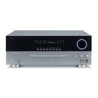
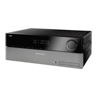
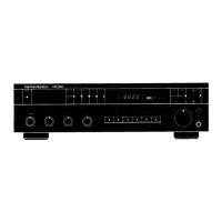
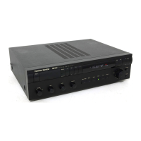
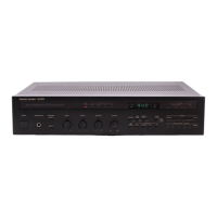
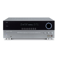
Detailed explanation of each button, knob, and display on the front panel.
Explanation of the indicators on the front panel information display.
Detailed explanation of each rear panel input and output connector.
Explanation of the functions of each button on the remote control.
A guide to diagnosing and resolving common operational issues.
Information on system memory and how to perform a processor reset.
Steps and values for adjusting amplifier bias for left and right channels.
Procedure to replace the volume encoder for volume control tracking issues.
Procedure for upgrading software to resolve silence during preset scan.
Instructions for removing the top cabinet cover.
Instructions for detaching the front panel assembly.
Instructions for removing the rear panel.
Instructions for removing the main printed circuit board.
Diagram showing the assembly of parts and a list of components.
Diagram illustrating the functional blocks and signal flow of the receiver.
Diagrams and dimensions detailing the physical size of the unit.
Details on the color and pattern of front panel illumination.
Table mapping front panel functions to grid assignments.
Reference to an example of external current amplifying connections.
Block diagram showing the internal structure and functions of the HVIST72F321R IC.
Diagram and pinout for the 64-pin TQFP package.
Detailed table of pin names, types, levels, port configurations, and functions.
Block diagram, signal names, and connection details for the EEPROM IC.
Overview of the dual operational amplifier's performance and characteristics.
Diagram of pin layout and equivalent circuit for the NJM2068.
Block diagram of the NJM2296M IC and associated components.
Block diagram, timing chart, and delay time definition for the voltage detector IC.
Pin configuration, description, and block diagrams for the reset IC.
Block diagram for the TC9164AF function/input IC.
Block diagram for the TC9163AF function/input IC.
Block diagram for the Toshiba TC9459F function/input IC.
Table detailing pin numbers, symbols, names, functions, and remarks.
Diagrams and pinouts for common transistor and regulator IC packages.
List of capacitors and resistors on the front PCB.
List of resistors used in the unit, with part numbers and specifications.
Diagram showing the layout of PCBs and their interconnections.
Diagram showing the placement of components and connectors on the main board.
Overall schematic of the receiver's electronic circuits.
Diagram showing the wiring and connections between major PCBs.
List and diagram of accessory items included with the manual.
Diagram showing how the unit is packaged for shipping.
| Speaker Load Impedance | 8 ohms |
|---|---|
| Input Impedance | 47k ohms |
| Tuner Type | AM/FM |
| Preset Stations | 30 |
| Power Output | 120 watts per channel |
| Frequency Response | 10Hz - 100kHz (+0dB, -3dB) |
| Total Harmonic Distortion | <0.07% at 20Hz – 20kHz |
| Dimensions | 440mm x 165mm x 410mm |
| Input Sensitivity | 200mV |
| Weight | 12.7kg |