--------------------------------------------------------HMCS47C,HMCS47CL
An
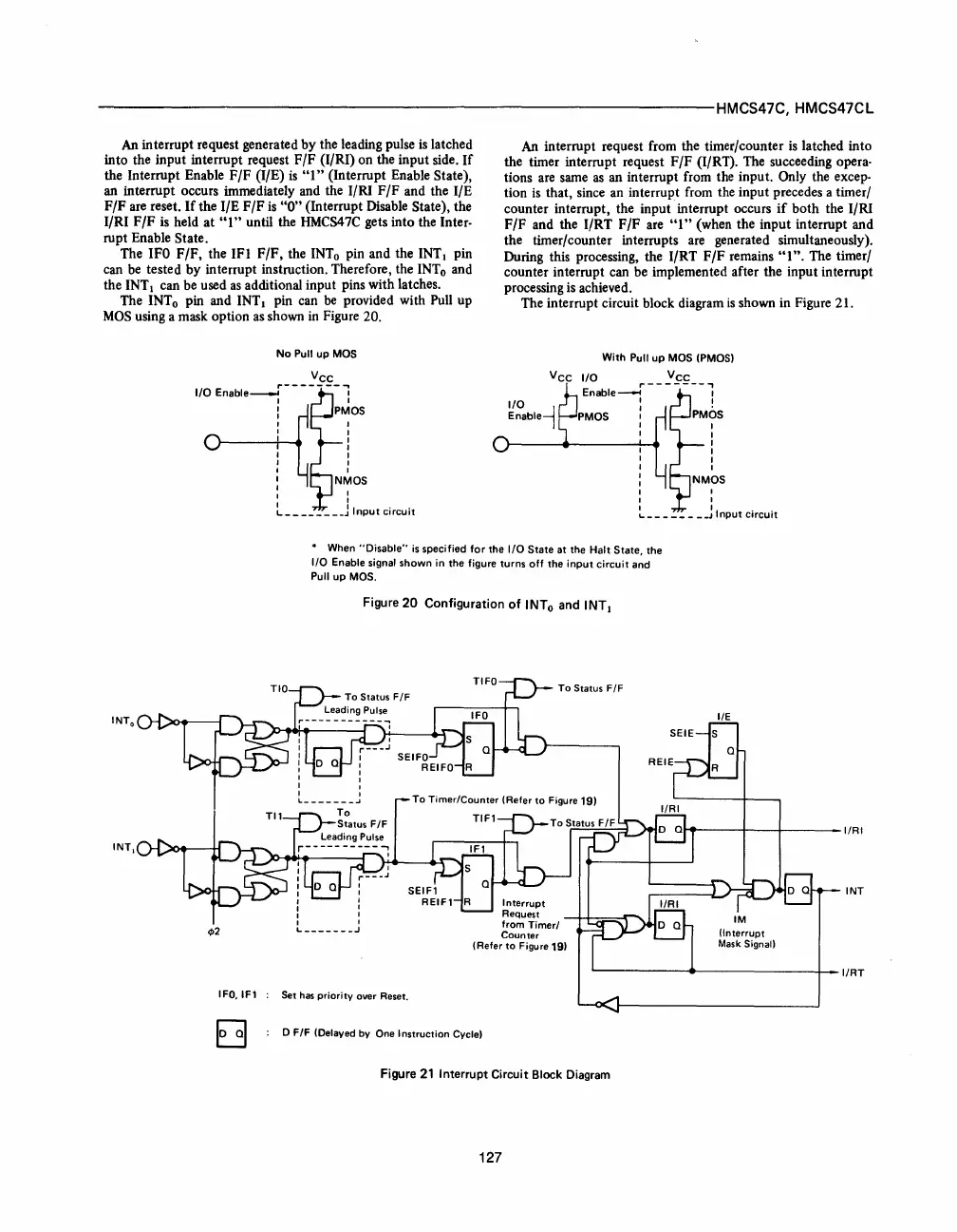
interrupt request generated by the leading pulse
is
latched
into the input interrupt request F/F (I/RI) on the input side. If
the Interrupt Enable F
/F
(I/E)
is
"I"
(Interrupt Enable State),
an interrupt occurs immediately and the I/RI
F/F
and the liE
F/F
are reset.
If
the liE F/F
is
"0"
(Interrupt Disable State), the
I/RI
F/F
is
held at
"I"
until the
HMCS47C
gets into the Inter-
rupt Enable State.
The
IFO
F/F, the IFI F/F, the
INTo
pin and the
INTI
pin
can
be
tested by interrupt instruction. Therefore, the
INTo
and
the INTI can
be
used
as
additional input pins with latches.
The
INTo
pin and INTI pin can
be
provided with Pull up
MOS
using a mask option
as
shown
in
Figure 20.
No
Pull
up
MOS
r----'!Ef-.,
I/O
Enable---'
I
I
PMOS
I
I
_______
.J
Input
circuit
An
interrupt request from the timer/counter
is
latched into
the timer interrupt request F/F (I/RT).
The
succeeding opera-
tions
are
same
as
an interrupt from the input. Only the excep-
tion
is
that, since
an
interrupt from the input precedes a timer/
counter interrupt, the input interrupt occurs
if
both the I/RI
F/F and the I/RT F
IF
are
"1"
(when the input interrupt and
the timerlcounter interrupts
are
generated simultaneously).
During this processing, the I/RT
F/F
remains
"1".
The timer/
counter interrupt can be implemented after the input interrupt
processing
is
achieved.
The interrupt circuit block diagram
is
shown in Figure 21.
Vee
I/O
With
Pull
up
MOS
(PMOS)
I
I
I I
I I
~
_______
.J
Input
circuit
* When
"Disable"
is
specified
for
the
I/O
State
at the
Halt
State,
the
I/O
Enable signal
shown
in
the
figure
turns
off
the
input
circuit
and
Pull
up
MOS.
IFO,IF1
Figure 20
Configuration
of
INTo
and
INTI
To
Status
F/F
liE
SEIE S
Q
REIE
R
~---I---l-----I/RI
(Interrupt
Mask
Signal)
INT
L-------~--------+__I/RT
Set
has
priority
over Reset.
D
F/F
(Delayed by One
Instruction
Cycle)
Figure
21
Interrupt Circuit Block Diagram
127
 Loading...

