HMCS47C,HMCS47CL--------------------------------------------------------
• RESET FUNCTION
The reset
is
perfonned by setting the RESET pin
to
"1"
("High" level) and the
HMCS47C
gets into operation by setting
it
to
"0"
("Low" level); Refer to Figure 22. Moreover, the
HMCS47C
has the power-on reset function (ACL; Built-in Reset
Circuit). The Built-in Reset Circuit restricts the
rise
condition
of
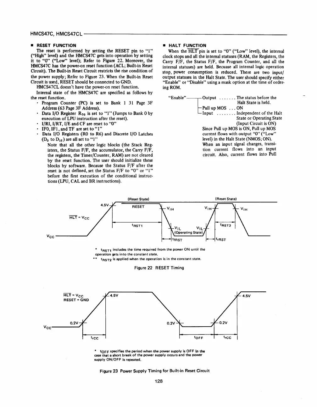
the power supply; Refer
to
Figure 23.
When
the Built-in Reset
Circuit
is
used, RESET should be connected
to
GND.
HMCS47CL
doesn't
have
the power-on reset function.
Internal state
of
the
HMCS47C
are specified
as
follows by
the reset function.
• Program Counter (PC)
is
set
to
Bank 1
31
Page
3F
Address (63
Page
3F
Address).
• Data I/O Register R,o
is
set
to
"1"
(Jumps
to
Bank 0 by
execution
ofLPU
instruction after the reset).
I/RI, I/RT, I/E and
CF are reset
to
''0''
•
IFO,
IFl,
and TF are set
to
"I"
Data I/O Registers
(RO
to
R6) and Discrete I/O Latches
(Do
to
DIS) are all set
to
"1"
Note that all the other logic blocks (the Stack
Reg-
isters, the Status F/F, the accumulator, the Carry FIF,
the registers, the Timer/Counter,
RAM)
are not cleared
by the reset function. The user should initialize these
blocks
by
software. Because the Status FIF after the
reset
is
not defined, set the Status
F/F
to
"0"
or
"1"
before the first execution
of
the conditional instruc-
tions
(LPU, CAL and BR instructions).
(Reset State)
RESET
Vee
-------'
• HALT FUNCTION
When
the HLT pin
is
set
to
"0"
("Low" level), the internal
clock stops and
all
the internal statuses (RAM, the Registers, the
Carry FIF, the Status FIF, the Program Counter, and all the
internal statuses)
are
held. Becuase
all
internal logic operation
stop, power consumption
is
reduced. There are two inputl
output statuses in the Halt State. The user should specify either
"Enable" or "Disable" using a mask option at the time
of
order-
ingROM.
"Enable"tOutput
.......
The status before the
Halt
State
is
held.
Pull up
MOS
...
ON
Input
........
Independent
of
the Halt
State or Operating State
(Input Circuit
is
ON)
Since
Pull up
MOS
is
ON, Pull up
MOS
current flows with output
"0"
("Low"
level) in the Halt State
(NMOS;
ON).
When
an input signal changes, transi-
tion current flows into
an
input
circuit. Also, current flows into Pull
• tRST1 includes
the
time required from
the
power
ON
until
the
operation gets
into
the
constant
state.
HLT=Vee
RESET = GND
O.2V
V
ee
-----"
tRST2
is
applied when
the
operation
is
in
the
constant
state.
Figure
22
RESET Timing
4.SV
•
tOFF
specifies
the
period when
the
power supply
is
OFF
III
the
case
that
a
short
break
of
the
power
supply occurs and
the
power
supply ON/OFF
is
repeated.
Figure 23 Power Supply Timing
for
Built-in
Reset
Circuit
128
4.SV
 Loading...

