---------------------------------
LCD-IV
When expansion
of
segment signal for liquid crystal display
is
designated by a program (Register
R42
="0"),
RI
is
used
as
a display data output terminal. This prohibits RI
to
be used
as
an I/O common channel by users (Refer
to
Figure 16, RI
channel).
If
LRA
or
LRB instruction
is
executed at the time, data
is
transferred
to
data I/O register, but the content
of
data I/O
register is not output from R
I.
If
LAR
or
LBR instruction
is
executed, display data
is
inputted
to
accumulator (A register)
or
B register.
Data
is
transferred from the accumulator
(A
register) and B
LRA.
LRB [
Instruction
~Mtr~IO"[
LAR.
LBR [
Instruction
-
-
One Instruction Cycle
/
\.
Rn
Output
Instruction
Rn
Pattern Genera-
tion
Instruction
R2.R3
register
to
data I/O registers
RI,
R2, and R3 through the bus
line. In addition,
ROM
bit patterns can be transferred
to
R2
and R3 by pattern generation instructions.
4-bit data can
be
inputted to the accumulator (A register)
and B register from
RO,
Rl
and
R2
channels
by
input instruc-
tions. However,
in
the case
of
I/O common channels
R2
and
R3, since data I/O register outputs are connected
to
terminals,
inputs are done to wired logic
of
register
output
and terminal
input information. For this reason, to input terminal input
signal, registers must be set
to
a state
that
would
not
affect
the terminal input.
(second cycle)
Rn
Input
Instruction
I--
Rn
Sampling
Pulse
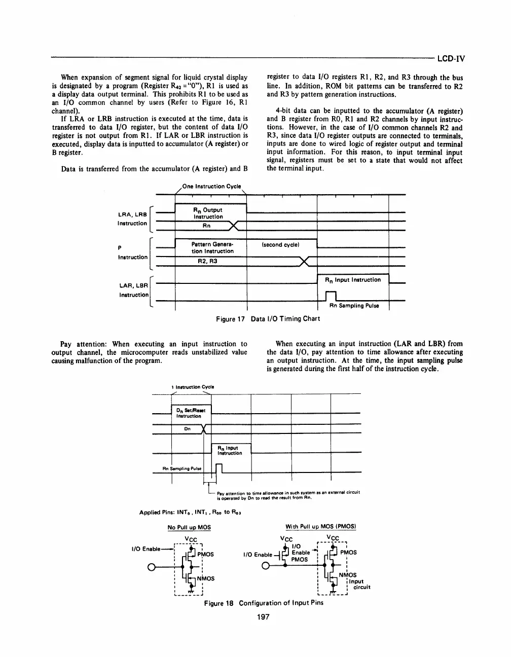
Figure
17
Data
I/O Timing Chart
Pay attention: When executing an input instruction
to
output channel, the microcomputer reads un stabilized value
causing malfunction
of
the program.
1 Inatructlon Cvcle
.....
On
Rn
Sampling Pulse
Rn
Input
Inatruction
When executing an input instruction (LAR and LBR) from
the data I/O, pay attention
to
time allowance after executing
an output instruction. At the time, the input sampling pulse
is
generated during the first half
of
the instruction cycle.
I T Pay attention
to
time allowance
in
such system as an external circuit
is
operated by On to read the result from Rn.
Applied Pins:
INTo.
INT
••
Roo
to
Ru
No Pull up MOS
VCC
I/O
E~'
!--t~---prs
: NMOS
, ,
: :
'-----
--~
With Pull
up
MOS
(PMOS)
Figure
18
Configuration
of
Input
Pins
197


 To Next Page
 Loading...