EasyManua.ls Logo

Hitachi AP1 - Page 200

Hitachi AP1
378 pages
Print Icon
To Next Page IconTo Next Page
To Previous Page IconTo Previous Page
Loading...
LCO-IY-------------------------------
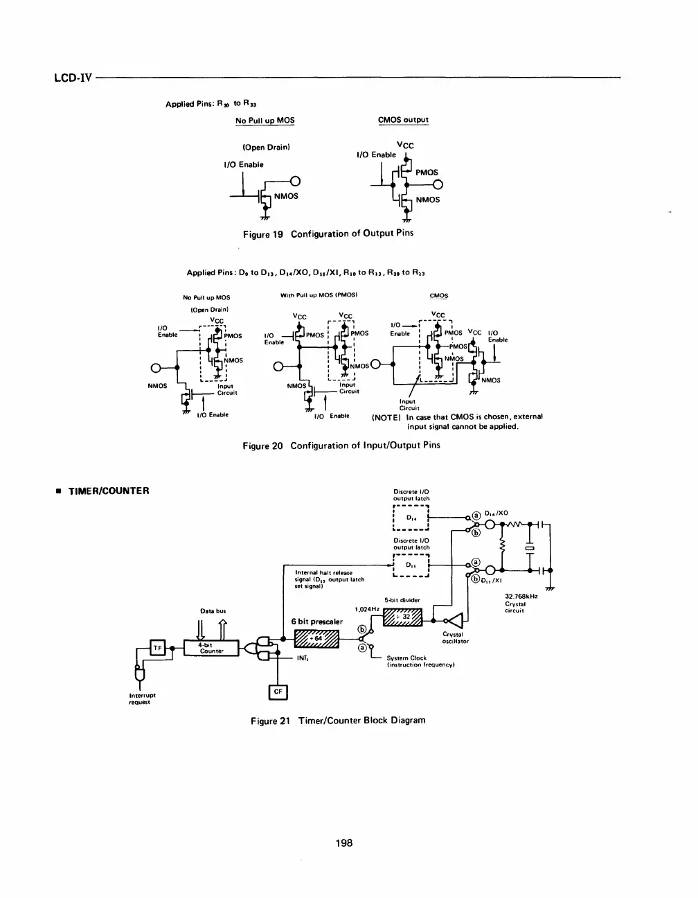
• TIMER/COUNTER
Applied Pins:
A30
to
Au
No Pull
up
MOS
CMOS
output
(Open Drain)
VCC
I~T~6
4~NM~
I/O Enable
~r-
Figure 19 Configuration
of
Output
Pins
Applied Pins:
Do
to
D
u
,
D,./XO,
DIS/XI, A
,o
to
Au,
Aoo
to
A,.
No Pull
up
MOS
10pen
Drain)
Vee
1/0
__
r-----~
Enable
:~.
MOS
I I
:
~MOS
I '
L
____
J
With Pull
up
MOS (PMOSI
Input
Circuit
ellll~
1/0
Enable
~
(NOTE)
In
case
that
CMOS
is
chosen, external
input
signal
cannot
be
applied.
Figure 20 Configuration
of
Input/Output
Pins
Discrete
1/0
output
latch
~-----1
, 0
"---n
t
___
I:_J-
Discrete
1/0
output
latch
,-----,
..-
________
--"
0..
...1
--+---CL\!
1 ,
Internal halt release
signal
(0
15
output
latch
set signal)
L
____
-'
Figure
21
Timer/Counter Block Diagram
198
32.768kHz
Crystal
circuit