LCO-IV------------------------------------------------------
__________
__
• Extension
of
Display Function
Number
of
display digits can be increased
by
externally con-
necting an
LCD driver LSI HD44100H
to
the LCD-IV.
The HD44100H consists
of
shift registers and latch and
liquid crystal drive circuit. When connected with the
LCD-IV,
the HD44100H is used
as
a circuit for segment. In the
LCD-
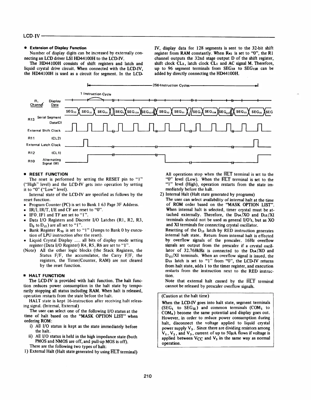
IV, display data for 128 segments
is
sent to the 32-bit shift
register from
RAM
constantly. When
R42
is
set
to
"0",
the
Rl
channel outputs the
32nd
stage
output
0
of
the shift register,
shift clock
CL2, latch clock CLI and
AC
signal
M.
Therefore,
up
to
96
segment terminals from
SEG33
to
SEGI28 can be
added by directly connecting the
HD44100H.
..
1.t-------------256-lnstruction
Cycles-------------.l.1
AI
_ Display
Channll-T
Data
R
13 Serial Segment
Data(D)
External
Shift
Clock
R11 (CL2)
External Latch
Clock
R12
R10
(CL1)
Alternating
Signal (M)
• RESET FUNCTION
1 I
nstruction
Cycle
,..c=::==-I II I
The reset
is
performed by setting the RESET pin
to
'.'
I"
("High" level) and the
LCD-IV
gets into operation by setting
it
to
"0"
("Low"
level).
Internal state
of
the LCD-IV are specified
as
follows by the
reset function.
• Program Counter (PC)
is
set to Bank I 63 Page 3F Address.
• IR/I, IR/T, I/E and CF are reset
to
"0".
•
IFO,IFI
and
TF
are set
to
"1".
• Data I/O Registers and Discrete I/O Latches
(RI,
R2, R3,
Do
to DIs) are
all
set
to
"1".
• Bank Register
R70
is
set to
"I"
(Jumps to Bank 0 by execu-
tion
of
LPU
instruction after the reset).
• Liquid Crystal Display .....
all
bits
of
display mode setting
register (Data
I/O Register) R4, RS, R6 are set
to
"I".
(Note)
All
the other logic blocks (the Stack Registers, the
Status
F/F,
the accumulator, the Carry
F/F,
the
registers, the Timer/Counter, RAM) are not cleared
by the reset function.
•
HALT
FUNCTION
The LCD-IV
is
provided with halt function. The halt func-
tion reduces power consumption in the halt state by tempo-
rarily stopping all status including RAM. When halt
is
released,
operation restarts from the state 'before the halt.
HALT state
is
kept 16-instruction after receiving halt releas-
ing signal. (Internal, External)
The user can select one
of
the following I/O status
at
the
time
of
halt based
on
the
"MASK OPTION LIST" when
ordering
ROM:
i)
AU
I/O status
is
kept
as
the state immediately before
the halt.
ii)
All
I/O status
is
held in the high impedance state
(both
PMOS
and
NMOS
are off, and pull-up
MOS
is
off).
There are the following two types
of
halt:
1) External Halt (Halt state generated by using HL T terminal)
I II
210
Sli
All
operations stop when the
HL
T terminal
is
set
to
the
"0"
level (Low).
When
the HLT terminal
is
set to the
"I"
level (High), operation restarts from the state
im-
mediately before the halt.
2) Internal Halt (Halt state generated by programs)
The user can select availability
of
internal halt
at
the time
of
ROM
order based on
the
"MASK OPTION LIST".
When internal halt
is
selected, timer crystal must be at-
tached externally. Therefore, the
DI4/XO and
Dis/XI
terminals should not be used
as
general I/O's,
but
as
XO
and
XI
terminals for connecting crystal oscillator.
Resetting
of
the
DIS
latch by RED instruction generates
internal haIt state. Return from internal halt
is
effected
by overflow signals
of
the prescaler. 16Hz overflow
signals are
output
from the prescaler
if
a crystal oscil-
lator
of
32.768kHz
is
connected
to
the DI4/XO and
DIS
/XI terminals. When an overflow signal
is
issued. the
015
latch
is
set to
"1"
from
"0",
the
LCD-IV returns
from halt state, adds 1
to
the timer register, and execution
restarts from the instruction next
to
the RED instruc-
tion.
Note
that
external halt caused by the HL T terminal
cannot be released by prescaler overflow signals.
(Caution
at
the halt time)
When the
LCD-IV goes into halt state, segment terminals
(SEG
I
to
SEG
32
) and common terminals
(COM
I
to
COM
4
)
become the same potential and display goes
out.
However,
in
order
to
reduce power consumption during
halt, disconnect
the
voltage applied
to
liquid crystal
power supply
V 3. Since there
ace
dividing resistors among
V I , V 2 , and V 3, current
of
up
to
SOIlA
flows
if
voltage
is
applied between
Vec
and
V3
in
the same way as normal
operation.


 To Next Page
 Loading...