---------------------------------LCD-IV
2. Status column shows the factor which affects status
by
the instruction of status change.
NZ
..........
ALU
Not
Zeto
C ..........
ALU
Overflow
in
Addition/Carry
NB
..........
ALU
Overflow
in
Subtraction/No Borrow
except above .... Content of status column affects status directly.
3. Carry flip-flop
is
not always affected
by
executing the instruction which affects the Status.
Instructions
which affect Carry flip·flop are eight
as
follows.
AMC
SEe
SMC
REC
DAA
ROTL
DAS
ROTR
4,
All
instructions except for P are executed
in
single
cycle.
P
is
executed
in
2 cycles.
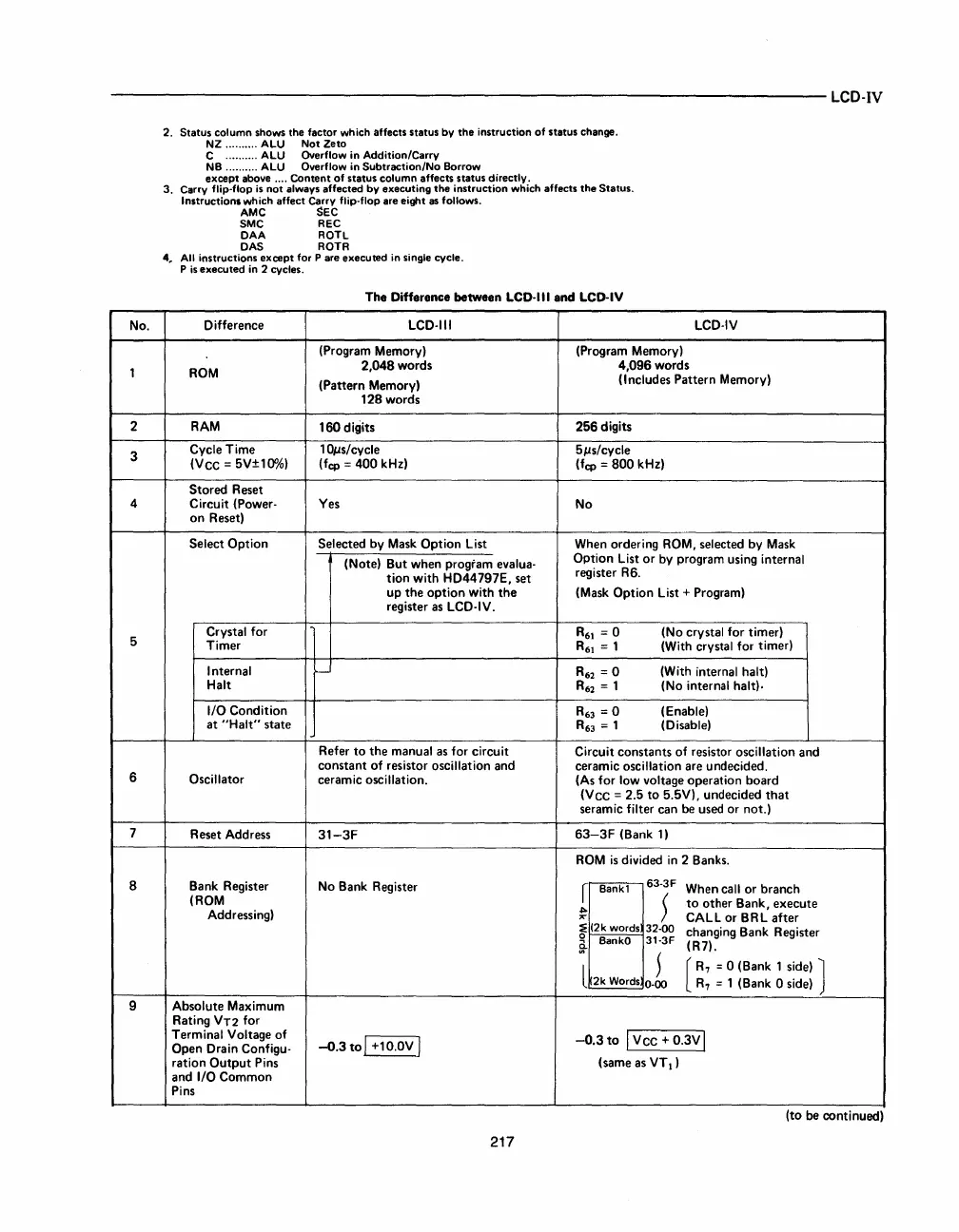
The
Difference
between
LCD-III
and
LCD-IV
No.
Difference
LCD-III LCD-IV
(Program Memory) (Program Memory)
1
ROM
2,048
words
4,096
words
(Pattern
Memory)
(Includes
Pattern
Memory)
128
words
2 RAM
160
digits
256
digits
3
Cycle
Time
lOlls/cycle
5lls/cycle
(VCC =
5V±1()otiJ)
(fcp =
400
kHz)
(fcp
=
800
kHz)
Stored
Reset
4
Circuit
(Power-
Yes
No
on
Reset)
Select
Option
Selected
by
Mask
Option
list
When ordering ROM, selected
by
Mask
(Note)
But
when
program
evalua-
OPtion
list
or
by
program
using internal
tion
with
HD44797E,
set
register R6.
up
the
option
with
the
(Mask
Option
List + Program)
register as
LCD-IV.
5
Crystal for
R6\
= 0
(No
crystal
for
timer)
Timer
R6\
= 1
(With crystal
for
timer)
Internal
"-
R62
= 0
(With internal halt)
Halt
R62
= 1
(No
internal halt).
I/O
Condition
R63
= 0
(Enable)
at
"Halt"
state
R63
= 1
(Disable)
Refer
to
the
manual as for
circuit
Circuit
constants
of
resistor
oscillation
and
constant
of
resistor oscillation
and
ceramic
oscillation
are
undecided.
6
Oscillator
ceramic
oscillation.
(As
for
low voltage
operation
board
(Vce
=
2.5
to
5.5Vl,
undecided
that
seramic filter
can
be used
or
not.)
7
Reset
Address
31-3F
63-3F
(Bank 1)
ROM
is
divided in 2 Banks.
8 Bank Register
No Bank Register
r~63-3F
When
call
or
branch
(ROM
~
)
to
other
Bank,
execute
Addressing)
CALL
or
BRL
after
:E
12k
words
32·00
changing Bank Register
~I
BankO
31·3F
(R7).
l 2k
Words
o.L
[R7
= 0 (Bank 1 side) J
--
R7
= 1 (Bank 0 side)
9
Absolute
Maximum
Rating VT2
for
Terminal
Voltage
of
-0.3
to
I +10.0V I
-0.3
to
I
Vee
+
0.3V
I
Open
Drain Configu-
ration
Output
Pins (same as
VT
\ )
and
I/O
Common
Pins
(to
be
continued)
217


 To Next Page
 Loading...