EasyManua.ls Logo

Hitachi AP1 - Page 220

Hitachi AP1
378 pages
Print Icon
To Next Page IconTo Next Page
To Previous Page IconTo Previous Page
Loading...
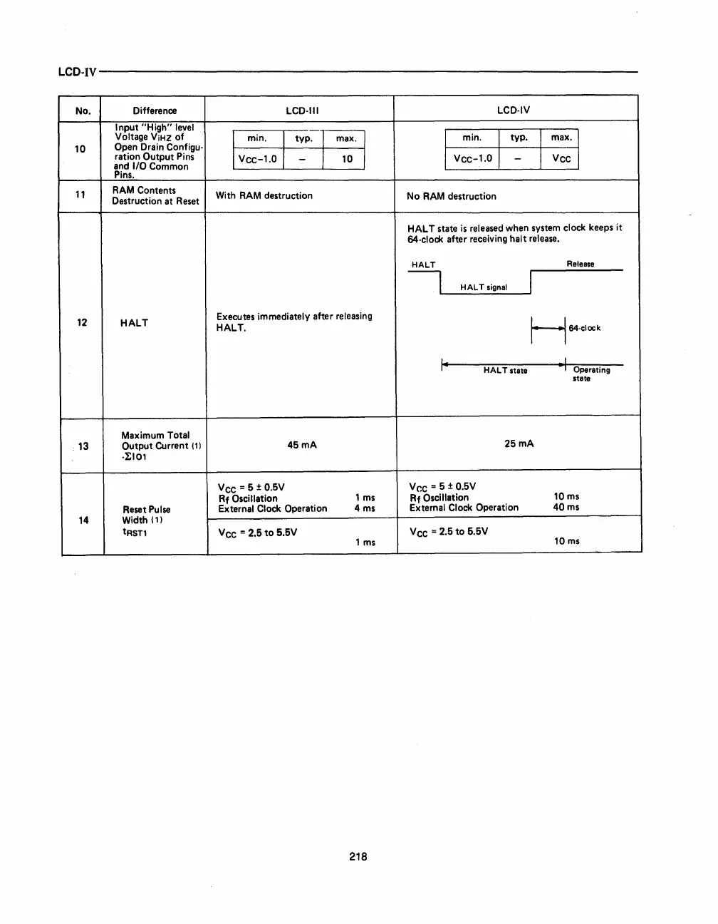
LCD-IV-------------------------------
No.
Difference
LCD·III
LCD-IV
Input
"High"
level
Voltage ViHZ
of
I
min.
I
typo
I
max·l
I
min.
I
typo
I
max.,
10
Open Drain Configu-
ration
Output
Pins
I
Vee-l.0
I
-
I
10
1
I
Vee-l.0
I
-
I
Vee
I
and 1/0 Common
Pins.
11
RAM Contents
With RAM destruction
No
RAM destruction
Destruction at
Reset
HAL
T state
is
released
when system clock keeps
it
64-clock after receiving
halt
release.
HALT
Release
I
HAL T
signal
I
12
HALT
Executes immediately after releasing
H64.CIOCk
HALT.
I·
HALT
state
·1
Operating
state
Maximum Total
13
Output
Current
(1)
45mA
25mA
·~I01
Vee
= 5 ± 0.5V
Vee
= 5 ± 0.5V
Rf
Oscillation
1
ms
Rf
Oscillation
10ms
Reset
Pulse
External Clock Operation
4
ms
External Clock Operation
40
ms
14
Width (1)
tRST1
Vee
= 2.5
to
5.5V
Vee
= 2.5
to
5.5V
1
ms
10
ms
218