HMCS«MC------------------------------------------------------------
• SERIAL INTERFACE
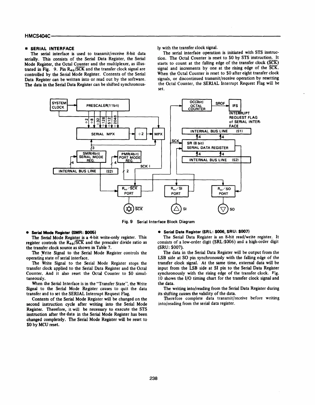
The serial interface
is
used to transmit/receive 8·bit data
serially. This consists
of
the Serial Data Register, the Serial
Mode Register, the
Octal Counter and the multiplexer,
as
illus·
trated in Fig. 9. Pin
~o/SCK
and the transfer clock signal are
controlled by the Serial
Mode
Register. Contents
of
the Serial
Data Register can be written into or read out by the software.
The data in the Serial Data Register can be shifted
synchronous·
ly with the transfer clock signal.
The serial interface operation
is
initiated with STS instruc·
tion. The Octal Counter
is
reset
to
$0 by
STS
instruction. It
starts to count at the falling
edge
of
the transfer clock (SCK)
signal and increments by one at the rising edge
of
the
SCK.
When
the Octal Counter
is
reset to $0 after eight transfer clock
signals, or discontinued transmit/receive operation by resetting
the
Octal Counter, the SERIAL Interrupt Request Flag
will
be
set.
Fig.9
Serial Interface Block Diagram
• Serill Mode Register
(SMR:
SOO5)
The Serial Mode Register
is
a 4·bit write-only register. This
register controls the
~o/SCK
and the prescaler divide ratio
as
the transfer clock source
as
shown in Table 7.
The
~rite
Signal to the Serial
Mode
Register controls the
operating state
of
serial interface.
The
Write
Signal
to
the Serial
Mode
Register stops the
transfer clock applied
to
the Serial Data Register and the Octal
Counter.
And
it
also reset the Octal Counter to $0 simul·
taneously.
When
the Serial Interface
is
in
the "Transfer State", the
Write
Signal to the Serial
Mode
Register causes to quit the data
transfer
and
to
set the SERIAL Interrupt Request
Flag.
Contents
of
the Serial Mode Register
will
be changed on the
second instruction cycle after writing into the Serial
Mode
Register. Therefore, it will be necessary to execute the
STS
instruction after the data in the Serial
Mode
Register has been
changed completely. The Serial
Mode
Register
will
be reset
to
$0
by
MCU
reset.
238
• Serill
Olte
Register (SRL: $006, SRU: $007)
The Serial Data Register
is
an 8-bit read/write register.
It
consists
of
a low·order digit (SRL:$OO6) and a high.order digit
(SRU: $007).
The data in the Serial Data Register
will
be output from the
LSB
side at
SO
pin synchronously with the falling edge
of
the
transfer clock signal. At the
same
time, external data will be
input from the
LSB
side at SI pin
to
the Serial Data Register
synchronously with the rising edge
of
the transfer clock.
Fig.
10 shows the I/O timing chart for the transfer clock signal and
the data.
The writing into/reading from the Serial Data Register during
its shifting causes the validity
of
the data.
Therefore complete data transmit/receive before writing
into/reading from the serial data register.


 To Next Page
 Loading...