EasyManua.ls Logo

Hitachi AP1 - Page 266

Hitachi AP1
378 pages
Print Icon
To Next Page IconTo Next Page
To Previous Page IconTo Previous Page
Loading...
HD614P080S---------------------------------------------------------------
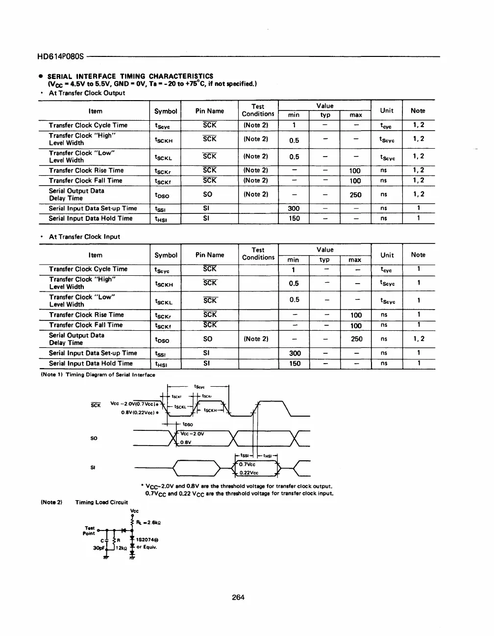
• SERIAL INTERFACE TIMING CHARACTERISTICS
(Vee
...
4.5V
to
5.5V,
GND =
OV,
Ta
-
-20
to
+75°C, if
not
specified.)
•
At
Transfer Clock
Output
Symbol
Test
Value
Item
Pin Name
Conditions
min
typ
Transfer Clock Cycle Time
t
Scvc
SCK
(Note 2)
1
-
Transfer Clock
"High"
tSCKH
SCK
(Note 2)
0.5
-
Level
Width
Transfer
Clock
"Low"
tSCKL
SCK
(Note 2)
0.5
-
Level
Width
Transfer
Clock Rise Time
tSCKr
SCK
(Note 2) -
-
Transfer Clock Fall Time
tSCKf
SCK
(Note 2)
-
-
Serial
Output
Data
toso
SO
(Note 2)
-
-
Delay Time
Serial
Input
Data Set-up Time
tSSI
SI
300
-
Serial
Input
Data Hold Time
tHSI
SI
150
-
•
At
Transfer Clock
Input
Test
Value
Item Symbol
Pin Name
Conditions
min
typ
Transfer Clock Cycle Time
t
Scvc
SCK
1
-
Transfer Clock
"High"
tSCKH
SCK
0.5
-
Level
Width
Transfer
Clock
"Low"
tSCKL
SCK
0.5
-
Level
Width
Transfer
Clock Rise Time
tSCKr
SCK - -
Transfer Clock Fall Time
tSCKf
SCK
-
-
Serial
Output
Data
toso
SO
(Note 2)
- -
Delay Time
Serial
Input
Data Set-up Time
tSSI
SI
300
-
Serial
Input
Data Hold Time
tHSI
SI
150
-
INote
11
Timing
Diagram
of
Serial Interface
5CK Vcc
-2.0VI0.7Vccl.
0.8VI0.22Vcc) •
50
51
H
tss,
-----c(
0.7Vcc
~____
O.22Vcc
""k
•
VCC-2.OV
and O.8V
are
the threshold voltage
for
transfer
clock
output.
(Note
21
O.
7V
CC
and 0.22
Vee
are
the threshold voltage
for
transfer
clock
input.
Timing
Load
Circuit
T
••
t
Point
Vcc
C R
1520749
~
RL_2'8kQ
30pF
12kQ
or Equiv.
264
Unit
Note
max
-
t
cvc
1,2
-
t
scvc
1,2
-
tScvc
1,2
100
ns
1,2
100
ns
1,2
250
ns
1,2
- ns 1
-
ns 1
Unit
Note
max
-
t
cvc
1
-
t
scvc
1
-
t
scvc
1
100
ns 1
100
ns 1
250
ns
1,2
-
ns
1
-
ns 1