--------------------------------------------------------------HD614P080S
• D-port
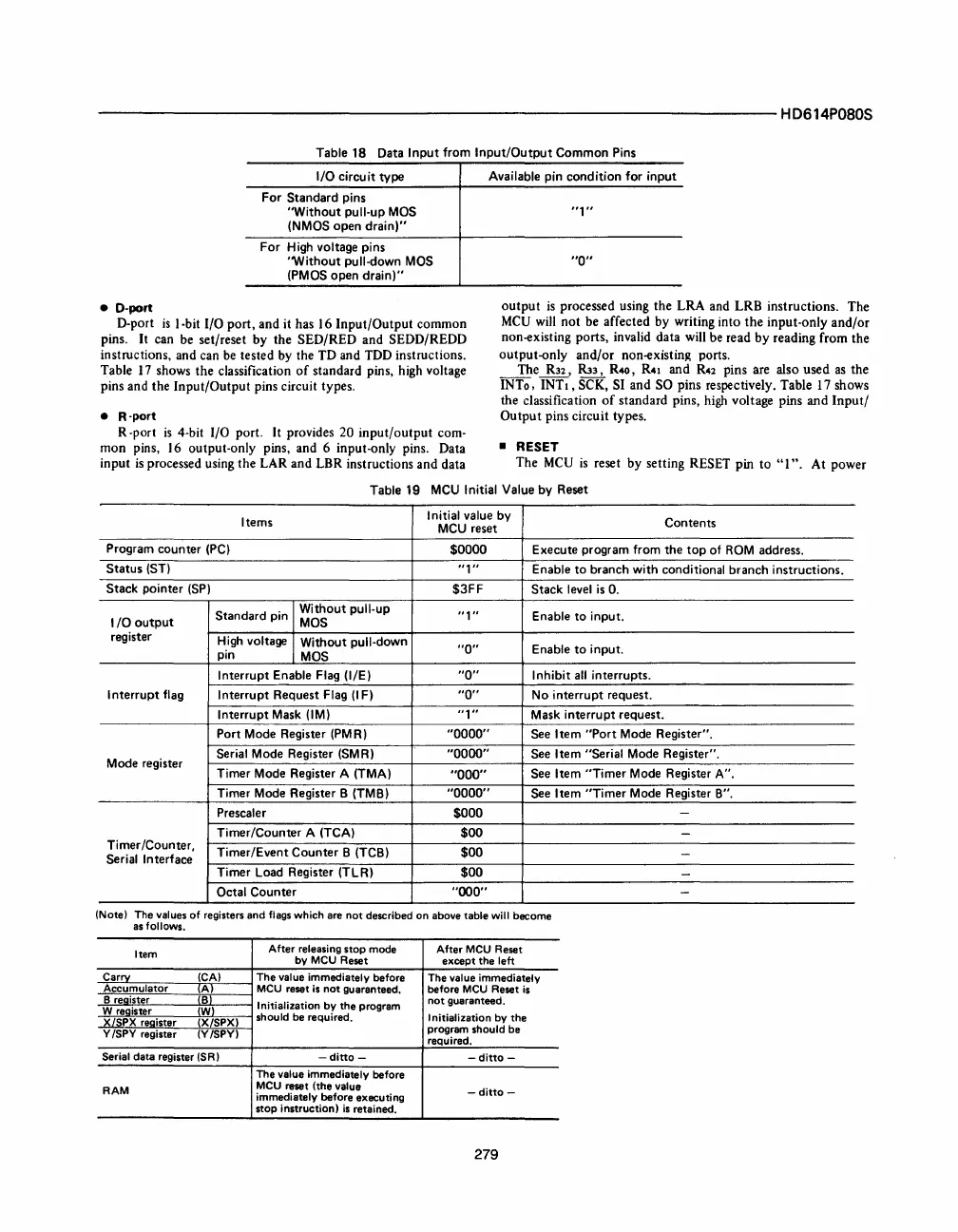
Table 18 Data
Input
from
Input/Output
Common Pins
I/O circuit
type
For Standard pins
"Without
pull-up
MOS
(NMOS open
drain)"
For High voltage pins
"Without
pull-down
MOS
(PMOS
open
drain)"
Available pin condition for input
"1"
"0"
D-port
is
I-bit I/O
port,
and
it has 16
Input/Output
common
pins.
It
can be set/reset
by
the SED/RED and SEDD/REDD
instructions, and can be tested by the TD and TDD instructions.
Table
17
shows
the
classification
of
standard pins, high voltage
pins and the
Input/Output
pins circuit types.
output
is
processed using the LRA and LRB instructions. The
MCV
will
not
be affected
by
writing into
the
input-only
and/or
non-existing ports, invalid data will be read
by
reading from the
output-only
and/or
non-existing ports.
The R32,
R33, R40,
R4I
and
R42
pins are also
used
as
the
INTo,
INTI,
SCK, SI and SO pins respectively. Table 17 shows
the classification
of
standard pins, high voltage pins
and
Input/
Output
pins circuit types .
• R-port
R-port
is
4-bit I/O port.
It
provides 20
input/output
com-
mon
pins, 16 output-only pins, and 6 input-only pins. Data
input
is
processed using
the
LAR
and
LBR instructions and data
• RESET
The
MCV
is
reset
by
setting RESET pin
to
"I".
At
power
Table 19
MCU
Initial Value by Reset
Items
Initial value
by
Contents
MCU
reset
Program counter
(PC)
$0000
Execute program from the
top
of
ROM
address.
Status
(ST)
"1"
Enable
to
branch with conditional branch instructions.
Stack pointer
(SP)
$3FF
Stack level
is
O.
Standard pin
Without pull-up
"1"
Enable
to
input.
I/O
output
MOS
register
High
voltage
Without pull-down
pin
MOS
"0"
Enable
to
input.
Interrupt Enable Flag (I/E)
"0"
Inhibit
all
interrupts.
Interrupt
flag
Interrupt Request Flag
(I
F)
"0"
No interrupt request.
Interrupt Mask
(1M)
"1"
Mask interrupt request.
Port Mode Register (PMR)
"0000"
See Item
"Port
Mode Register".
Serial
Mode Register (SMR)
"0000"
See Item "Serial Mode Register".
Mode register
Timer Mode Register A (TMA)
"000"
See Item
"Timer
Mode Register A".
Timer Mode Register B
(TMB)
"0000"
See Item
"Timer
Mode Register
B".
Prescaler
$000
-
Timer/Counter A (TCA)
$00
-
Timer/Counter,
Timer/Event
Counter B (TCB)
$00
-
Serial Interface
Timer Load Register (TLR)
$00
-
Octal Counter
"000"
-
(Note) The values
of
registers and flags which
are
not
described on above table
will
become
as
follows.
Item
After
releasing stop mode
After
MCU Reset
by
MCU Reset
except the
left
Carry (CA)
The
value immediately before
The
value immediately
Accumulator
(A)
MCU reset
is
not
guaranteed.
before MCU Reset
is
B reaister
B
Initialization
by
the program
not
guaranteed.
W register
(W)
X/SPX register (X/SPX)
should
be required.
Initialization
by
the
Y
/SPY register (Y/SPY)
program should be
required.
Serial data register (SR)
-
ditto-
-
ditto-
The value immediately before
RAM
MCU reset (the value
-ditto
-
immediately before executing
stop instruction)
is
retained.
279


 To Next Page
 Loading...