HD614P080S---------------------------------------------------------------
ON
or recovering from stop mode, apply RESET input more
than
tRC
to obtain the necessary time for oscillator stabiliza·
tion.
In
other cases, the MeV reset requires at least two instruc·
tions cycle time
of
RESET input.
Table
19
shows initialized items by MeV reset and each
status after reset.
OSC
I
[>
Oscillator
OSC.
<l
•
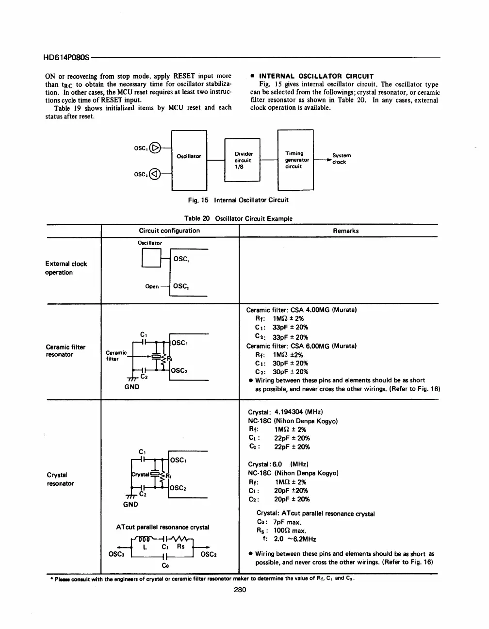
INTERNAL
OSCILLATOR CIRCUIT
Fig.
15
gives
internal oscillator circuit. The oscillator type
can
be
selected from the followings; crystal resonator, or ceramic
fIlter resonator
as
shown in Table 20. In any cases, external
clock operation
-is
available.
Divider
circuit
1/8
Timing
generator
circuit
System
clock
Fig. 15 Internal Oscillator Circuit
External clock
operation
Ceramic
filter
resonator
Crystal
resonator
Table
20
Oscillator Circuit Example
Circuit
configuration
Oscillator
OSCI
Open
OSC.
CI
ceramicfc::::::l
filter
C2
GND
OSCI
OSC2
GND
ATcut
parallel
resonance
crystal
~~
OS~~
OSC2
Co
Remarks
Ceramic
filter: CSA 4.00MG (Murata)
Rf:
lMn
±2%
Cl:
33pF ±
20%
C~:
33pF ±
20%
Ceramic
filter:
CSA 6.00MG (Murata)
Rf:
lMn
±2%
Cl:
30pF ±
20%
C2: 30pF ±
20%
• Wiring between
these
pins
and
elements should
be
as
short
as
possible,
and
never
cross
the other wirings. (Refer
to
Fig. 16)
Crystal: 4.194304 (MHz)
NC·18C (Nihon Denpa Kogyo)
Rf:
lMn
±
2%
Cl
: 22pF ±
20%
Cz
: 22pF ±
20%
Crystal: 6.0 (MHz)
NC·18C (Nihon Denpa Kogyo)
Rf:
lMn
±
2%
Cl
: 20pF ±20%
C2
: 20pF ±
20%
Crystal:
AT
cut parallel
resonance
crystal
Co: 7pF max.
Rs:
lOOn
max.
f:
2.0
......
6.2MHz
• Wiring between
these
pins
and
elements should
be
as
short
as
possible, and never
cross
the other wirings. (Refer
to
Fig. 16)
•
PI
...
conlUlt with the engineers of crystal or ceramic filter resonator maker
to
determine the value of Rf, C
I
and C
•.
280



 To Next Page