EasyManua.ls Logo

Hitachi AP1 - Page 344

Hitachi AP1
378 pages
Print Icon
To Next Page IconTo Next Page
To Previous Page IconTo Previous Page
Loading...
HMCS404CL--------------------------------------------------------------------------
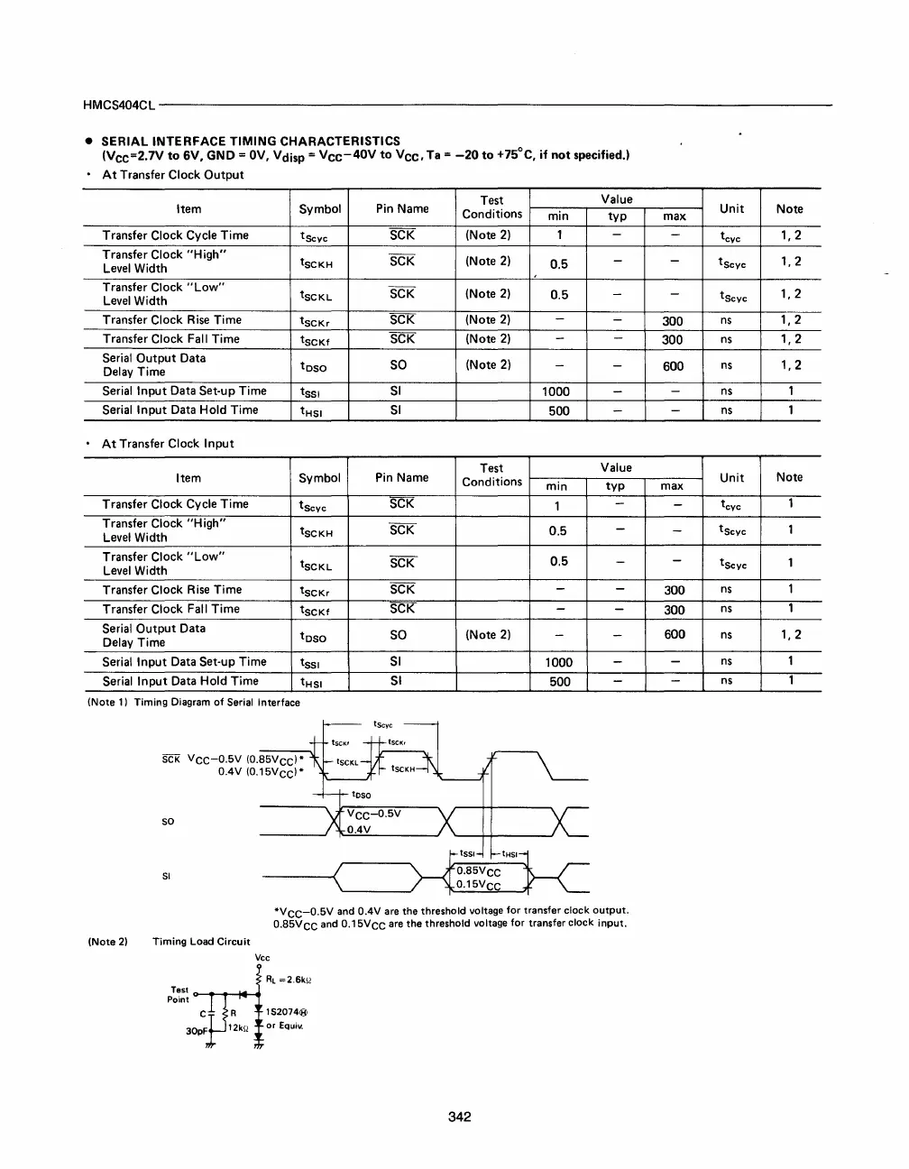
• SERIAL INTERFACE TIMING CHARACTERISTICS
(VCC=2.7V
to
6V, GND =
OV,
Vdisp =
Vec-40V
to
Vee,
Ta =
-20
to
+7SoC, if
not
specified.)
•
At
Transfer Clock
Output
Item Symbol
Transfer Clock Cycle Time
ts
eve
Transfer Clock
"High"
tSCKH
Level
Width
Transfer
Clock
"Low"
tSCKL
Level
Width
Transfer
Clock Rise Time
tSCKr
Transfer Clock Fall Time
tSCKf
Serial
Output
Data
toso
Delay Time
Serial
Input Data Set-up Time
tSSI
Serial Input Data Hold Time
tHSI
•
At
Transfer Clock Input
Item
Symbol
Transfer
Clock Cycle Time
ts
eve
Transfer Clock "High"
tSCKH
Level Width
Transfer
Clock
"Low"
tSCKL
Level
Width
Transfer
Clock Rise Time
tSCKr
Transfer Clock Fall Time
tSCKf
Serial
Output
Data
toso
Delay Time
Serial
Input Data Set-up Time
tSSI
Serial
Input
Data Hold Time
tHSI
(Note
1)
Timing
Diagram
of
Serial Interface
SCK
VCC-O.5V
(O.85VcC)*
OAV
(O.15VcC)*
so
Pin Name
Test
Conditions
min
SCK
(Note
2)
1
SCK
(Note
2)
0.5
SCK
(Note
2)
0.5
SCK
(Note
2)
-
SCK
(Note
2)
-
SO
(Note
2)
-
SI
1000
SI
500
Test
Pin Name
Conditions
min
SCK
1
SCK
0.5
SCK
0.5
SCK
-
SCK
-
SO
(Note
2)
-
SI
1000
SI
500
ts
cvc
SI
H
tss,
tHSI}-c
____
----«
O.85VCC
'-____
O.15VCC
Value
typ
-
-
-
-
-
-
-
-
Value
typ
-
-
-
-
-
-
-
-
*VCC-O.5V
and O.4V are the threshold voltage
for
transfer
clock
output.
O.85VCC and O.15VCC
are
the threshold voltage
for
transfer
clock
input.
(Note
2)
Timing
Load
Circuit
Vee
lS2074(j3)
or
Equiv.
342
Unit
max
Note
-
t
eve
1,2
-
t
seve
1,2
-
t
seve
1,2
300
ns
1,2
300
ns
1,2
600
ns
1,2
-
ns
1
-
ns
1
Unit
Note
max
-
t
eve
1
-
t
seve
1
-
t
seve
1
300
ns
1
300
ns
1
600
ns
1,2
-
ns
1
-
ns
1