EasyManua.ls Logo

Hitachi AP1 - Page 347

Hitachi AP1
378 pages
Print Icon
To Next Page IconTo Next Page
To Previous Page IconTo Previous Page
Loading...
-----------------------------------------------------------------------HMCS404CL
o
15
16
63
64
4095
4096
16383
l
I
Vector Address
Zero-Page Subroutine
(64Words)
Program
Pattern
(4096Words)
•
RAM
MEMORY
MAP
$0000
0_
JMPL
Instruction.
_
1
(Jump
to
RESET
Routine)
$OOOF
2_
JMPL Instruction
-
$0010
(Jump to
INTo
Routine)
3
\
4
JMPL
Instruction
5-
(Jump
to
i1iii1
Routine)
-
6 JMPL Instruction
$ 003F
$0040
7 - (Jump
to
TIMER-A Routine) -
8
JMPL
Instruction
-
-
9
(Jump
to
TIMER-B Routine)
10
11
$OFFF
121-
JMPL
Instruction.
_
$1000
13
(Jump
to
SERIAL
Routine)
14
$3FFF
15
Fig.
1
ROM
Memory
Map
$0000
$0001
$0002
$0003
$0004
$0005
$0006
$0007
$0008
$0009
$OOOA
$OOOB
$OOOC
$0000
$OOOE
$
OOOF
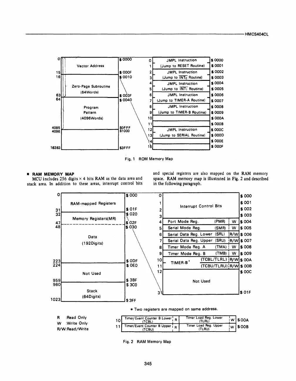
MeU includes 256
digits
x 4 bits
RAM
as
the
data
area
and
stack
area.
In
addition to
these
areas,
interrupt control bits
and
special
registers
are
also
mapped
on
the
RAM
memory
space.
RAM
memory
map
is
illustrated
in
Fig.
2
and
described
in
the
following
paragraph.
o
31
32
RAM-mapped Registers
Memory Registers(MR)
$000
$01F
$020
\
0
1
Interrupt Control Bits
2
3
4
Port Mode
Reg.
(PMR)
:W
47
48
----------------
----
$ 02F
$
000
$001
$002
$003
$004
$
005
$006
$
007
$008
$
009
$OOA
$OOB
$OOC
223
224
959
960
1023
Data
(192Digits)
Not
Used
Stack
(64Digits)
R
:Read
Only
W :Write Only
R/W: Read/Write
$030
5
Serial Mode
Reg.
(SMR)
IW
6
Serial Data
Reg.
Lower
(SRL)
!R/W
7
Serial Data
Reg.
Upper
(SRU)
:R/W
8
Timer Mode
Reg.
A
(TMA)!
W
9 Timer Mode
Reg.
B
(TMB)
I W
$ODF
10_
TIMER-B·
(TCBLlTLRL) :
R/W
$OEO
11
(TCBU/TLRU):
R/W
12
$
3BF
Not Used
$
3CO
31
$ 01F
$3FF
* Two registers are mapped
on
same address.
Timer
Load
Reg.
Lower
10~~~--~~--~~_+~~~T~im-e-r~L~~!~~~~~~~~~.u~p-p-er--~-i$00A
11
(TLRU)
$
OOB
Fig.
2
RAM
Memory
Map
345