HMCS45C,HMCS45CL-------------------------------------------------------
•
Accumulator
(A; A Register) and
Carry
F/F
(C)
The result
of
the Arithmetic
Logic
Unit (ALU) operation
(4
bits) and the overflow
of
the ALU are loaded into the accumula-
tor and the Carry F/F. The Carry
F/F
can be set, reset or tested.
Combination of the accumulator and the Carry
F/F
can be right
or left rotated. The accumulator
is
the main register for ALU op-
eration and the Carry
F/F
is
used to store the overflow generated
by
ALU operation when the calculation
of
two
or more digits
(4
bits/digit)
is
performed.
• 8 Register (8)
The result
of
ALU operation
(4
bits)
is
loaded into this regis-
ter. The B register
is
used
as
a sub-accumulator to stack data
temporarily and also used as a counter.
• X Register
IX)
The result
of
ALU operation
(4
bits)
is
loaded into this regis-
ter. The X register has exchangeability for the
SPX
register. The
X register addresses the RAM
file
and
is
composed
of
4-bit regis-
ter.
• SPX
Register
(SPX)
The SPX register has exchangeability
for
the X register.
The SPX register
is
used to stack the X register and expand
the addres3ing system
of
RAM
in
combination with the X regis-
ter.
It
is
composed
of
4-bit register.
• Y Register (Y)
The result
of
ALU operation
(4
bits)
is
loaded into this regis-
ter. The Y register has exchangeability
for
the
SPY
register. The
Y register can calculate itself simultaneously with transferring
data by.the bus lines, which
is
usable
for
the calculation
of
two
or more digits
(4
bits/digit). The Y register addresses the RAM
digit and I-bit Discrete I/O.
•
Spy
Register
(SPY)
The
SPY
register has exchangeability for the Y register. The
SPY
register
is
used to stack the Y register and expand the ad-
dressing system
of
RAM and I-bit Discrete I/O in combination
with the Y register.
• INPUT/OUTPUT
•
4-bit
Data
Input/Output
Channel
(R)
Output Function
r - - - - - - - -
--,
D~
(
2
3
22
21
2
0
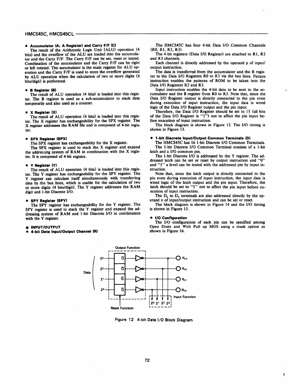
The HMCS45C has four 4-bit Data
110
Common Channels
(RO,
Rl,
R2, R3).
The 4-bit registers (Data
110
Register) are attached to
Rl,
R2
and
R3
channels.
Each channel
is
directly addressed
by
the operand p
of
input/
output instruction.
The data
is
transferred from the accumulator and the B regis-
ter to the Data I/O Registers
RO
to
R3
via
the bus lines. Pattern
instruction enables the patterns
of
ROM
to be taken into the
Data
110
Registers
R2
and
R3.
Input instruction enables the 4-bit data to be sent to the
ac-
cumulator and the B register from
RO
to
R3.
Note that, since the
Data
110
Register output
is
directly connected to the pin even
during execution of input instruction, the input data
is
wired
logic
of
the Data
110
Register output and the pin input.
Therefore, the Data
110
Register should be set
to
15
(all bits
of
the Data 110 Register
is
"1")
not to affect the
pin
input be-
fore execution
of
input instruction.
The block diagram
is
shown
in
Figure
12.
The
110
timing
is
shown
in
Figure
13.
•
1-blt
Discrete
Input/Output
Common
Terminals
(D)
The HMCS45C has
16
I-bit Discrete
110
Common Terminals.
The I-bit Discrete
110
Common Terminal consists
of
a I-bit
latch and a
110
common pin.
The I-bit Discrete
110
is
addressed
by
the Y register. The ad-
dressed latch can be set or reset
by
output instruction and
"0"
and
"1"
a level can be tested with the addressed pin
by
input in-
struction.
Note that, since the latch output
is
directly connected to the
pin even during execution
of
input instruction, the input data
is
wired
logic
of
the latch output and the pin input. Therefore, the
latch should be set to
"1"
not to affect the pin input before ex-
ecution
of
input instruction.
The
Do
to
D3
terminals are also addressed directly
by
the op-
erand n
of
input/output instruction and can be set or reset.
The block diagram
is
shown
in
Figure
14
and the
110
timing
is
shown
in
Figure
15.
•
I/O
Configuration
The
110
configuration
of
each pin can be specified among
Open Drain and With Pull up
MOS
using a mask option as
shown
in
Figure
16.
Rn3
Rn2
Rnl
Rno
Figure
12
4-bit
Data
I/O
Block Diagram
72
 Loading...

