------------------------------------------------------HMCS45C,HMCS45CL
Table 3 Timer Range
Specified
Number
of
Specified
Number
of
Time (ms)
Time (ms)
Value cycles
Value cycles
0
1,024
10.24
8
512
5.12
1
960
9.60
9
448
4.48
2
896
8.96
10
384
3.84
3
832
8.32
11
320
3.20
4
768
7.68
12
256
2.56
5
704
7.04
13
192
1.92
6
640
6.40
14
128
1.28
7
576
5.76
15
64
0.64
[NOTE] Time
is
based
on instruction frequency 100kHz. (one instruction cycle
=1
Ops)
Figure 18 The Pulse
Width
of
the INT, pin
in the Counter Mode
• INTERRUPT
The HMCS45C can be interrupted
in
two
different
ways:
through the external interrupt input pins
(~NTo,
INTI) and the
timer/counter interrupt request. When any mterrupt occurs, pro-
cessing
is
suspended, the Status
F/F
is
unchanged, the present
program counter
is
pushed onto the stack STl and the contents
of the stacks
STl,
ST2
and
ST3
are pushed onto the stacks ST2,
ST3
and ST4 respectively. At that time, the Interrupt Enable
F/F
(I/E)
is
set and the address jumps to a fixed destination (Inter-
rupt Address), and then the interrupt routine
is
executed.Stack-
ing the registers other than the program
co~nter
must be
p~r
formed
by
the program. The interrupt routme must end
Wit?
RTNI (Return Interrupt) instruction which sets the
liE
F/F
SI-
multaneously with the RTN instruction.
The Interrupt Address:
Input Interrupt Address
.....
1 Page 3F Address
Timer/Counter Interrupt Address
.....
o Page 3F Address
The input interrupt has priority over the timer/counter inter-
rupt.
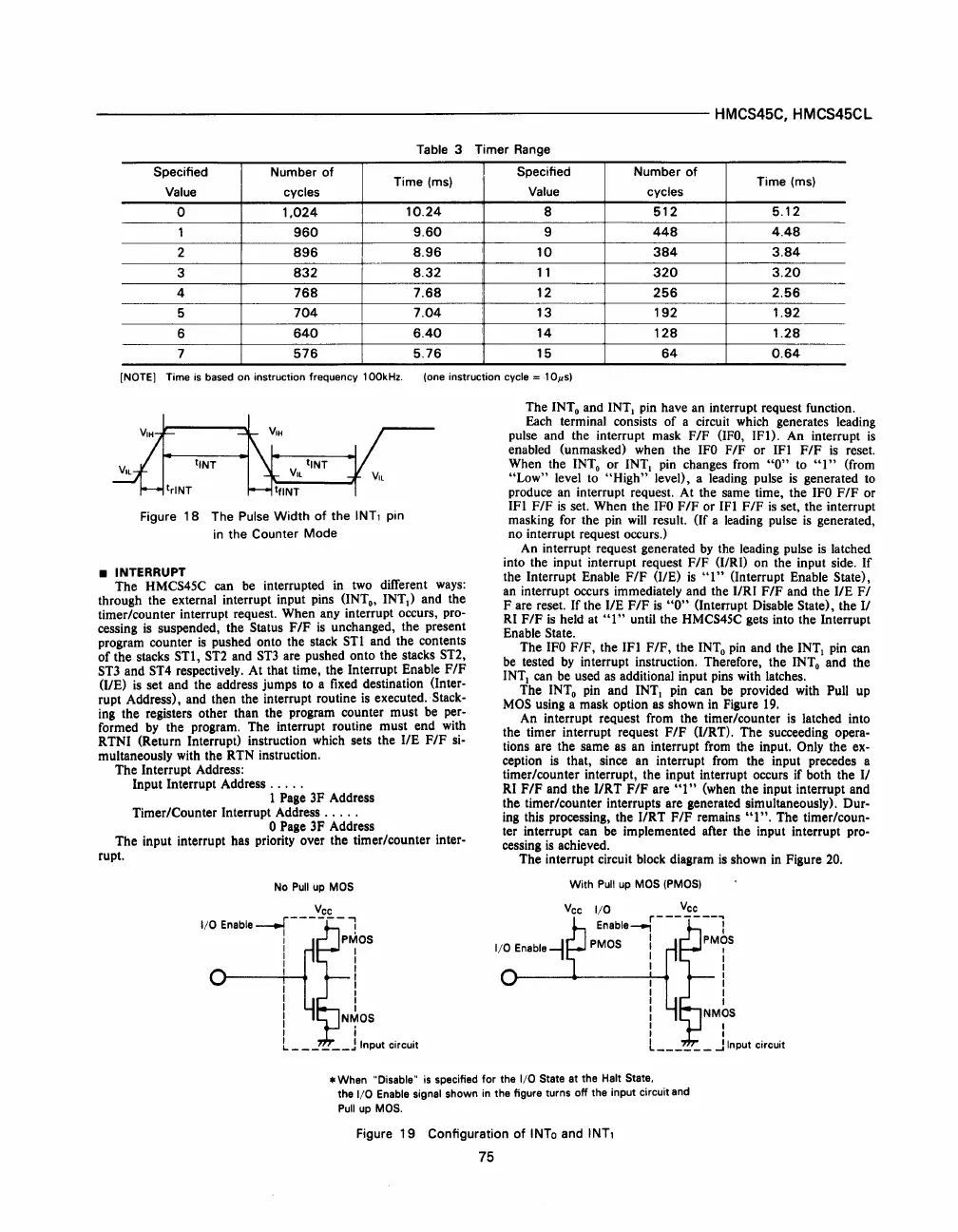
No
Pull
up MOS
The
INTo
and
INTI
pin have an interrupt request function.
Each terminal consists of a circuit which generates leading
pulse and the interrupt mask
F/F
(IFO,
1Ft). An interrupt
is
enabled (unmasked) when the
IFO
F/F or IFI
F/F
is
reset.
When the
INTo
or INT.
pin
changes from
"0"
to
"I"
(from
"Low"
level to
"High"
level), a leading pulse
is
generated
to
produce an interrupt request. At the same time, the
IFO
F/F
or
IFI
F/F
is
set. When the
IFO
F/F or IFI F/F
is
set, the interrupt
masking for the
pin
will
result. (If a leading pulse
is
generated,
no interrupt request occurs.)
An interrupt request generated
by
the leading pulse
is
latched
into the input interrupt request
F/F (IIRI) on the input side. If
the Interrupt Enable
F/F
OlE)
is
"I"
(Interrupt Enable State),
an interrupt occurs immediately and the IIRI F/F and the
liE
FI
F are reset. If the
liE
F/F
is
"0"
(Interrupt Disable State), the II
RI
F/F
is
held at
"I"
until the HMCS45C gets into the Interrupt
Enable
State.
The
IFO
F/F, the IFI F/F, the
INTo
pin
and the INT. pin can
be
tested
by
interrupt instruction. Therefore, the
INTo
and the
INT. can be used
as
additional input
pins
with latches.
The
INTo
pin
and INT.
pin
can
be
provided with Pull
up
MOS
using a mask option as shown
in
Figure
19.
An interrupt request from the timer/counter
is
latched into
the timer interrupt request
F/F
(I/RT).
The succeeding opera-
tions are the same
as
an interrupt
from
the input. Only the ex-
ception
is
that, since an interrupt
from
the input precedes a
timer/counter interrupt, the input interrupt occurs if both the
II
RI
F/F
and the IIRT
F/F
are
"I"
(when the input interrupt and
the timer/counter interrupts are generated simultaneously). Dur-
ing this processing, the IIRT
F/F
remains
"I".
The timer/coun-
ter interrupt can be implemented after the input interrupt pro-
cessing
is
achieved.
The interrupt circuit block diagram
is
shown
in
Figure
20.
With
Pull
up
MOS (PMOS)
Vcc
,
,
______ J Input circuit
* When "Disable"
is
specified for the I/O State at the Halt State.
the
I/O
Enable signal shown
in
the figure turns off the input circuit and
Pull
up
MOS.
Figure
19
Configuration
of
INTo and INT,
75
 Loading...

