HMCS46C,HMCS46CL--------------------------------------------------------
I (Page Part)
~
Bank Part
{\
r--
Page Part
~;----
Address Part
~
(Data
for
Modification)
~
~.=
:1=
:0
I C I
B,
:
B.
: B
I
:
Bo
I
A,
:
A.:
AI
:
Ao
I
r-"-T-T-T-T-T-T-,-"T-"T-'--'
(Reference I
PC
II
I PC
IO
PC. I PC. I PC, I PC, I
BIB
I A I A I A I A I
ROM address) L
+~
•
..1
~~
1
+~0..1..
+:
.J.
+~~
+~
• ..L
_1..1
_0..L
_'
.J.
_'.L
_I
.....
_0.J
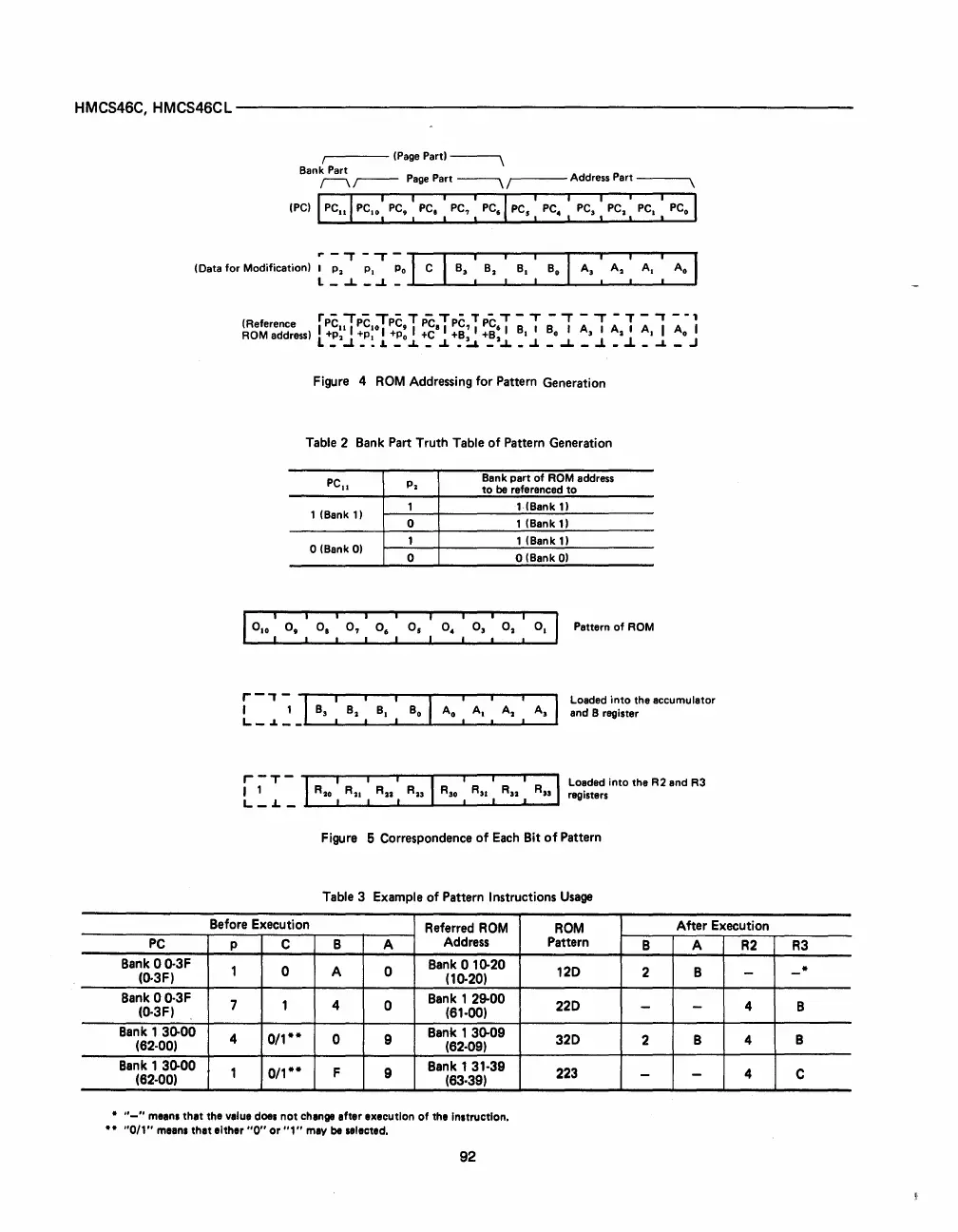
Figure 4 ROM Addressing
for
Pattern Generation
Table 2 Bank Part Truth Table
of
Pattern Generation
PC
11
p.
Bank
part
of
ROM address
to
be referenced
to
1 (Bank
1)
1
1
(Bank
11
0
1 (Bank
11
o (Bank
01
1 1 (Bank
11
0
o (Bank
01
I
0.
0
:
o. : o. :
0,
:
0,
: 05 : 0 4 : 0
3
:
O.
:
O.
I Pattern
of
ROM
Loaded
into
the
accumulator
and
B register
[~:
~
"'I,-R-'-OT:-R-.-.
r:
-R-"-':-R-u-,,r--R-30.,:r-R-,-.T:-R-3-'
r:
-R-
,
",I
;~~::~sinto
the
R2
and
R3
Figure 5 Correspondence
of
Each
Bit
of
Pattern
Table 3 Example
of
Pattern Instructions
Usage
Before Execution
Referred ROM
ROM
After
Execution
PC
p
C B
A
Address
Bank
00·3F
1
0
A 0
Bank
010-20
(0·3F)
(10·20)
Bank
00·3F
7
1 4
0
Bank 1 29-00
(0·3F)
(61·00)
Bank
130-00
4
0/1**
0
9
Bank 1
30-09
(62·00)
(62·09)
Bank 1 30-00
1
0/1**
F
9
Bank 1 31·39
(62·00)
(63·39)
•
"-"
meens
thet
the
velue
doel
not
chenge
after
axecutlon
of
tha
Instruction.
••
"0/1"
means
thet
either
"0"
or
"1"
mev be selected.
92
Pattern
B
A
R2
120
2 B
-
220
-
-
4
320
2
B
4
223
-
-
4
R3
*
-
B
B
C
 Loading...

