Do you have a question about the Hitachi HMA-6500 and is the answer not in the manual?
Specifies the continuous RMS power output of the amplifier at 8 ohms.
Details harmonic distortion and frequency response characteristics.
Specifies input parameters and compatible speaker impedance ranges.
Lists available power supply voltages, frequencies, and consumption.
Provides the physical dimensions and weight of the amplifier.
Instructions for removing the main cover and escutcheon assembly.
Procedure for removing the Power MOS FET components from the unit.
Important safety precautions for handling the unit's high-capacity power supply.
Guidance on proper installation of parts to maintain product safety and integrity.
Explanation of the DC amplifier's coupling switch function and purpose.
Details the role and connection of resistor R1 in the signal path and chassis ground.
Procedure for adjusting the idle current of the amplifier with no signal.
Steps to adjust the output DC offset after input DC adjustment is complete.
Procedure for adjusting the input DC offset with the unit warmed up.
How to adjust the sensitivity of the power output meters.
Procedure to verify the normal operation of the ASO detection circuit for Power MOS FETs.
How to confirm the proper functioning of the speaker protection relay circuit.
Instructions on how to test Power MOS FETs using a tester.
Explains the muting, speaker DC voltage, and Power MOS FET ASO protection circuits.
Highlights the design for low distortion and wide frequency response using MOS FETs.
Describes the DC amplifier's NFB loop and its benefits for accurate power transmission.
Explains the protection circuits for Power MOS FETs and DC voltage detection.
Schematic representation of the main amplifier's printed wiring board components and connections.
Detailed layout of components and terminal numbers on the main amplifier PWB.
Illustrations of power supply board component placement for various regional configurations.
Details the capability to connect and use two pairs of speakers.
Details the built-in current mirror and DC voltage detection circuits for protection.
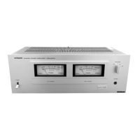
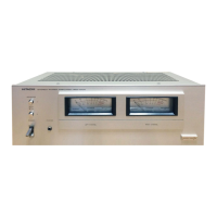
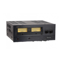
Describes the large power meters for accurate output level and channel balance monitoring.
List of replacement capacitors for the main amplifier printed wiring board.
List of replacement resistors for the main amplifier printed wiring board.
List of replacement semiconductor components for the main amplifier PWB.
List of replacement diodes for the main amplifier printed wiring board.
List of various other replacement parts including switches, jacks, and holders.
List of parts required for the dial mechanism assembly.
List of parts for the rear plate assembly.
List of parts for the final assembly of the unit.
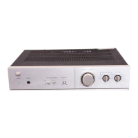
Identifies and describes the function of each component on the front and rear panels.
| Signal-to-Noise Ratio | 120dB (A-weighted) |
|---|---|
| Frequency Response | 5Hz to 100kHz |
| Total Harmonic Distortion | 0.01% (DC) |
| Input Sensitivity | 1.5V |
| Dimensions | 430 x 170 x 430 mm |
| Weight | 25 kg |