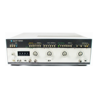
Model 214B
SERVICE BLOCK 4
OUTPUT BOARD
A1
THEORY
OF
OPERATION
The
output
board
A 1 can be divided into 4 main
functional
blocks:
-
input
Schmitt
trigger
-
duty
cycle
detect/overload
detect
-
amplitude
vernier and overload switch
-
output
amplifier
Each
of
these
blocks
is
described
in
the
following paragraphs.
Input Schmitt Trigger
The
input
Schmitt
trigger comprises:
-
transformer
T401,
which isolates potentials
of
the
output
amplifier
from
the
timing
board,
and also differentiates
the
timing
circuit
output
pulse.
emitter
follower
0400,
which isolates
the
transformer T401
from
the
following
Schmitt
trigger.
Schmitt
trigger
0401
/
0402.
A positive pulse
at
the
base
of
0401
causes Q401 to c
ut
o
ff
, and
0402
conducts.
This stable
conditions
exists until
the
next
negative pulse arrives
from
0400
which switches
0401
on
and
0402
off.
The
duty
cycle
detect
signal
is
derived
from
the
0401
collector and
routed
to
the
overload
detection
circuit.
To
ensure
that
integrator charge-up (in the overload
detect
circuit)
is
determined
only
by
the
duty
cycle
of
the
detect
signal (and
not
amplitude),
the
amplitude
is
clamped
to
approx.
3.5
V by
CR400
and
VR400
.
Overload Detection/Overload Switch/Amplitude Vernier
Theduty
cycle
detect
signal derived
from
0401
collector
is
inverted by
0421
and
limited
by
CR424.
Pulses at
the
collector
of
0421
are
then
integrated by R447 and C416. With increasing
duty
cycle
at
the
base
of
0421,
the
voltage across C416 decreases (switching
0421
on
causes C416
to
discharge).
Shou
Id
the
C416 voltage decrease
to
a
point
where it
is
lower
than
the
reference voltage
at
U401 a/
pi
n 2,
the
output
voltage
of
comparator
U401 a
is
switched
to
a minimum. (The
threshold
voltage
at
comparator
U401 changes according
to
amplitude
range
due
to
the
varying
duty
cycle limits i.e. 10 %
in
30-100
V
range :
50
%
in
all
other
ranges. I n
the
30
-
100
V
amplitude
range,
K403
switches
the
0425
base
to
-155
V,
thus turning
Q425
off. U401a
threshold
is
then
determined
by
R448
/ R449.
In
all
other
amplitude
ranges,
0425
is
turned
on,
resistors
R450
/ R451
then
being
connected
in
parallel with R449,
thus
lowering
the
U401 a
threshold).
With U401a
output
switched
to
minimum,
C419
is
discharged via
CR427,
which
in
turn
switches
U401b
/
pin 7
to
maximum
output
(OVERLOAD LED on).
0426
switches
on
(via
CR428,
R464) and transistors
0427
/
0428
switch off, causing
approximately
-
155
V
to
be applied
to
the
grids
of
tubes
V401,
V402.
This negative voltage
at
0428
collector
is
also applied
to
the
bases
of
0406
/
0407
(0416
/
0417)
via
R413/
R414
(R428
/ R427). Transistor
0407
(0417)
turns
off and
0406
(0416)
turns
on,
switching -
155
V
to
the
gates
of
F ET's
0408
/
0418.
With negative voltages at
the
tube
grids and F
ET
gates,
the
output
amplifier
is
disabled (i.e.
no
output
current).
Service
8-29
Scans by ArtekMedia => 2009