Section
Vlll
THEORY OF OPERATION
Model
3455A
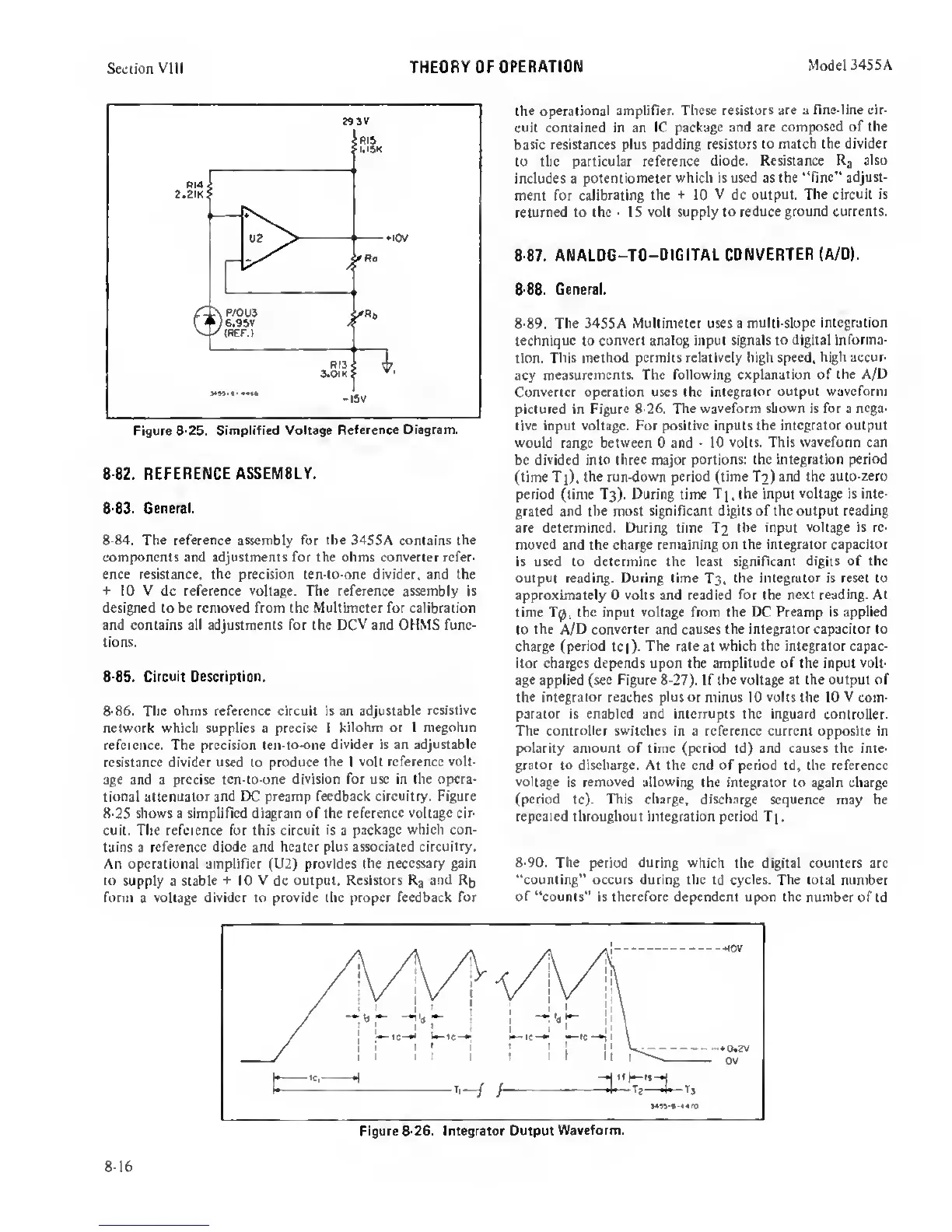
Figure
8-25. Simplified Voltage
Reference Diagram.
8-82. REFERENCE ASSEMBLY.
8-83. General.
8-84. The reference assembly for the
3455A
contains
the
components and adjustments for the ohms converter refer*
ence resistance, the precision cen-to-one divider, and the
+
10 V dc reference voltage. The reference assembly is
designed to be removed from the Multimeter for calibration
and contains all adjustments for the DCV and OHMS func-
tions.
8-85.
Circuit
Description.
8-86.
The ohms reference circuit is an adjustable
resistive
network which supplies a precise 1
kilohm or
I
megohm
reference. The precision
ten-to-one divider is an adjustable
resistance divider used to produce
the
1
volt reference volt-
age and a precise
ten-to-one division for use in the opera-
tional attenuator
and DC
preamp feedback circuitry. Figure
8-2S
shows
a
simplified diagram of the reference
voltage
cir-
cuit. The reference for this circuit is a
package which con-
tains a reference
diode
and
heater plus associated
circuitry.
An operational amplifier (U2)
provides the necessary gain
to supply a stable
-t-
10
V
dc
output. Resistors
Ra
and
Rb
form
a
voltage divider to provide the proper feedback
for
the
operational amplifier. These
resistors are
a
fine-line cir-
cuit contained in an IC
package and are
composed of the
basic
resistances plus padding resistors
to match the divider
to the particular
reference diode. Resistance
Ra
also
includes a
potentiometer which is used as the
“fine” adjust-
ment for calibrating
the
+
10 V dc output.
The circuit is
returned
to the
•
15 volt supply to
reduce ground currents.
8-87. ANALOG-TO-OIGITAL
CONVERTER (A/D).
8-88.
General.
8-89. The 34SSA Multimeter uses a
multi-slope integration
technique
to
convert analog input signals to
digital informa-
tion. This
method permits relatively high speed,
high accur-
acy
measurements. The following explanation of
the A/D
Converter operation uses the
integrator output waveform
pictured in Figure
8-26. The waveform
shown
is for a
nega-
tive input voltage. For positive inputs
the integrator output
would range
between
0 and
-
10
volts. This waveform can
be
divided into three
major
portions: the integration
period
(lime
Ti),
the run-down period (time
T2)
snd the auto-zero
period (lime T3). During time Tj
,
the input voltage is inte-
grated
and
the most significant digits of the output reading
are determined. During time T2 the input
voltage is re-
moved
and the
charge remaining on the integrator capacitor
is used to determine the least significant
digits of the
output reading. During time
T3,
the integrator is
reset
to
approximately 0 volts and readied for the
next reading.
At
time T0, the input
voltage
from
the DC Preamp
is
applied
to
the A/D converter
and
causes the integrator capacitor to
charge (period
tci
). The rate
at
which the integrator capac-
itor charges depends upon the amplitude of the input
volt-
age
applied (see Figure 8-27).
If
the voltage
at
the output of
the integrator
reaches plus or minus 10
volts
the 10 V com-
parator is enabled and interrupts the inguard controller.
The
controller
switches in a reference current opposite
in
polarity amount of time (period td) and causes the inte-
grator to discharge. At the end of period td, the reference
voltage
is
removed allowing
the integrator to again charge
(period
tc).
This charge, discharge
sequence may be
repeated throughout integration period
T].
8-90.
The
period
during
which the digital counters are
“counting” occurs during the td
cycles.
The total number
of “counts” is therefore dependent upon the number
of td
8-16
 Loading...