Model 345SA SERVICE GROUP
A
Section VIII
a.
Check
for a clock signal at A10U26 pin
27.
If no signal exists or the signal
level
is
below
4 V
(peak
to
peak), troubleshoot the inguard clock
circuit.
b. Check the ± 10
V
reference
voltages
at AI0TP8 for + 10
V
± 100
/tV.
and at A10TP7 for-IO V
±
20 mV
(schematic 5).
If these voltages
are too
low,
the 34SSA may not complete the Auto-Cal
routine and lock up.
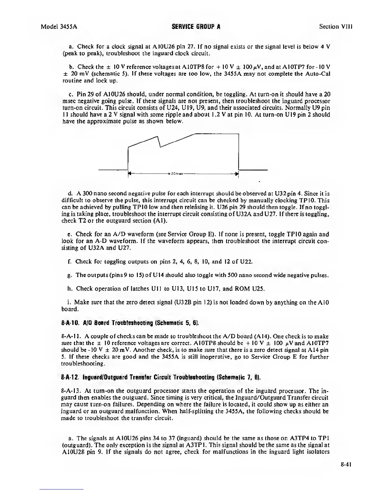
c. Pin
29 of A10U26 should, under normal condition, be toggling. At
tum-on it should
have
a 20
msec
negative
going pulse. If these signals are not present, then troubleshoot the inguard processor
turn-on circuit. This circuit consists of U24, U19, U9, and their associated circuits. Normally U9 pin
11 should
have
a 2
V signal with
some ripple and about 1.2
V
at pin 10. At turn-on UI9 pin 2 should
have the approximate pulse as shown below.
d. A 300 nano second negative pulse for each interrupt should
be
observed
at U32 pin
4.
Since it is
difHcult
to
observe the pulse,
this
interrupt circuit can be checked
by manually clocking TP 10. Utis
can be
achieved
by pulling TPIO
low
and then releasing it. U26 pin 29 should then toggle. If
no toggl-
ing is taking place, troubleshoot the interrupt circuit consisting of U32A and U27. If there is toggling,
check T2 or the outguard section (Al).
e. Check for an
A/D waveform
(see
Service
Group E). If none is present, toggle TPIO again and
look for an
A-D waveform.
If the
waveform
appears, then troubleshoot the interrupt circuit con-
sisting of
U32A
and U27.
f. Check
for toggling
outputs on pins
2, 4, 6, 8, 10,
and 12 of U22.
g.
The outputs (pins 9 to IS) of U14 should also toggle
with
500 nano second wide negative pulses.
h. Check operation of latches
Ull to UI3,
UlS
to U17, and
ROM
U2S.
i. Make sure that the zero detea signal (U32B pin
12)
is not loaded down
by anything
on
the AIO
board.
8-A-10.
AID Board Troubloahooting (Schamatic
5,
61.
8-A-l 1 . A couple of checks can be made
to
troubleshoot the A/D
board
(A14).
One check is to make
sure that the ± 10 reference
voltages
are correa. A10TP8 should be 10 V
±
100 and A10TP7
should be
•
10
V
±
20 mV.
Another check, is to
make
sure that there is a zero detect signal at A14 pin
S. If these checks are good and the 34SSA is still inoperative,
go
to Service Group E for further
troubleshooting.
8-A-12. InguardlOutguard Transfer Circuit Troublashooting (Schamatic
7,
8).
8-A-I3. At turn-on the outguard processor starts the operation of
the inguard
processor.
The in-
guard
then
enables
the outguard. Since timing is
very
critical, the Inguard/Outguard Transfer circuit
may
cause turn-on
failures.
Depending
on
where
the
failure
is located, it could
show
up as either an
inguard or
an outguard malfunaion. When
half-splitting the 34S5A, the
following
checks should be
made to troubleshoot the transfer circuit.
a. The
signals
at
A10U26 pins 34 to
37
(inguard) should be the same as those on A3TP4 to TPI
(outguard). The only exception is the signal at
A3TP
1 . This signal should be the same
as
the
signal
at
A10U28 pin
9.
if
the signals do not agree, check for malfunctions in the inguard light isolators
8-41
 Loading...