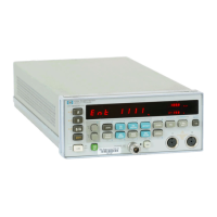
Model
4328A
LLst
of
Tables
List
of
Illustration
LIST
OF
TABLES
Number
Title
Page
1-1.
3-1.
3-2.
5-l.
5-2
5-3.
5-4.
5-5.
5-6.
5-7.
6-L
Specifications
......
, .
1-2
Characteristics
of
Applied
Current
on
Samples
and
Maximum
Power
Dtssipation
..............
,.
. .
..
. .
3-5
Ma..ximum
Values
of
Resistance
and
Length
of
Lead
Wire
.......
, _ .
..
. .
3-7
Recommended
Test
Equipment
....
,
...
5-1
Linearity
Test
............
,
..
,
......
5-2
Full
Scale
Test
,
..............
,
...
, .
5-2
Power
Supply
Test
..........
_.
. . . _
..
5-3
Out-of-Circuit
Transistor
Resistance
Measurements
...........
,
.........
5-6
Safe
Ohmmeter
Range
for
Transistor
Resistance
Measurements
5-6
Etched
Circuit
Soldering
Equipment
..
,
5-7
Ltst
of
Reference
Designators
and
Abbreviations
.....
,
...
, . . . ,
........
6-1
Number
Title
6-2.
7-1.
8-1.
8-2.
8-3.
8-4.
8-5.
8-6.
8-7.
8-8.
8-9.
8-10.
Reference
Designation
Index
.......
,
..
Backdating
Changes
..
,
.....
,
.....
.
4328A
Overall
Troubleshootmg
....
.
Oscillator
P/0
A3
Troubleshooting
.
Schmitt
Trigger
P,'O
A3
Troubleshooting
,
..........
_
....
, -
Flip-Flop
P/0
A3
Troubleshooting
.
Limitter
P/0
A3
Troubleshooting
. ,
....
AC
Amplifier
P/0
A2
Troubleshooting
..
,
...........
.
Phase
Detector
and
DC
Amplifier
P
/0
A2
Troubleshooting
.
Modulator
P iO A2
Troubleshooting
Power
Supply
Troubleshooting
....
,
..
,
Ni-Cd
Power
Supply
Troubleshooting
..
Page
6-2
7-1
8-5
8-7
8-7
8-9
8-9
8-11
8-11
8-11
8-13
8-15
LIST
OF
ILLUSTRATIONS
Number
Title
Page
1-1.
3-1.
3-2.
3-3.
3-4.
3-5.
3-6.
3-7.
3-8.
3-9.
4-1.
4-2.
4-3.
4-4.
4-5.
4-6.
4-7.
5-l.
5-2.
5-3.
7-1.
7-2.
8-1.
8-2.
8-3.
8-4.
8-5.
8-6.
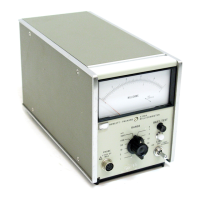
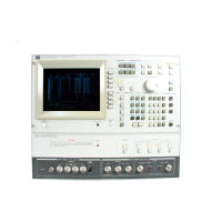
Model
4328A
Milhohmmeter
. . . . . . . . . .
1-1
Front
Panel
Controls
and
Connectors
. .
3-2
Rear
Panel
Controls
and
Connectors...
3-3
Operating
Procedure
. . . . . . . . . . . . . . . .
3-4
Probe
Combmation
.....
, . . . . . . . . . . . .
3-5
Probe
Installation
......
,.
. . . . . . . . . . . .
3-6
16005A
Clip-type
Probes
. . . . . . . . . . . . .
3-6
16006A
Pin-type
Probes
..•....
,
......
3-6
16007A
1
B
Test
Leads
................
3-6
4-Terminal
Device
Measurement....
. .
3-7
Basic
Low
Resistance
Measurement
...
4-1
SimphfLed
Block
Diagram,.......
. . . . . .
4-1
Operation
of
Phase
Detector
....
_ . . . . .
4-2
Model
4328A
Oscillator
Talking
Schematic
....
, . . . . . . . . . . . . . . . . . . .
4-5
Model
4328A
Phase-Sensitive
Amphher
Talking
Schematic
. . . . . . .
4-7
Model
4328A
Power
Supply
Talking
Schematic
....
, _
.....
,
............
4-9
Model
4328A
Ni-Cd
Power
Supply
....
.
Talking
Schematic
. . . . . . . . . . . . . . . .
4-11
Transistor
Biasing
CharacteristLcs
...
,
5-4
(0.
9m.f2
+ j 1.
8m0)
Impedance
.........
5-7
(900
+ J 180Q)
Impedance
..
,
..........
5-7
Partial
Schematic
of
A2
Ass'y
. . . . . . . .
7-1
Parhal
Schematic
of
A3
Ass'y
........
7-2
Schematic
Diagram
Notes...
. . . . . . . . . .
8-2
Overall
Block
Diagram.
. . . . . . . . . . . . . .
8-3
Model
4328A
Waveforms
. . . . . . . . . . . . .
8-4
Model
4328A
Waveform
Test
Point
Locations
. . . . . . . . . . . . . . . . . . . . . . . .
8-5
Model
4328A
Left
Internal
VIew . . . . . . .
8-6
Model
4328A
Bottom
Internal
V'lew . . . .
8-6
Number
Title
Page
8-7.
8-8.
8-9.
8-10.
8-11.
8-12.
8-13.
8-14.
8-15.
8-16.
8-17.
8-18.
8-19.
8-20.
8-21.
Model
4328A
Rear
Internal
View
........
8-8
Model
4328A
Right
Internal
View
.......
8-10
Model
4328A
Top
lnternal
View
.......
8-10
Model
4328A
Power
Supply
PC
Board
...
8-12
Model
4328A
Ni-Cd
Power
Supply
PC
Board
.........................
8-14
Oscillator
Assembly
A3
Component
Locations
........................
8-16
Range
Switch
Assembly
A4
Component
Locations
..............
8-16
Oscillator
Assembly
A3
Schematic
.....
8-17
Range
Switch
Assembly
A4
Schematic
..
8-17
Mother
Board
Assembly
A5
Schemattc
..
8-17
Phase
Sensittve
Amplifier
Assembly
A2
Component
Locations
.....•..•..
8-18
Mother
Board
Assembly
A5
Component
Locations
..............
8-18
Phase
Sensitive
Amplifier
Assembly
A2
Schematic
............
,
.......
8-19
Mother
Board
Assembly
A5
Schematic
...•......•..........•..
8-19
Power
Supply
Assembly
Al
..........
.
Component
Locations
..............
8-20
Power
Supply
Assembly
Al
Schematic
........................
8-21
Mother
Board
Assembly
A5
Schematic
...........
,
............
8-21
Ni-Cd
Power
Supply
Assembly
A6
Component
Locations
..............
8-22
Mother
Board
Assembly
A5
Schematic
_
.........
_
.......
_
.....
8-23
Ni-Cd
Power
Supply
Assembly
A5
Schematic
. . . . . .
...........
,
......
8-23
iii