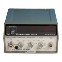
9E-5-27. 1300 MHz Channel Troubleshooting
9E-5-28. Set the RESOLUTION switch to 1 kHz and
the RANGE switch to A. Supply a 100 MHz, 25-millivolt,
sinusoidal input to the channel and perform the following
ste
s.
9E-5-29. Both Channels Inoperative
9E-5-30. Set RESOLUTION switch to 1 Hz position,
RANGE switch to B, and apply 1 MHz sinusoidal input to
the 100 MHz channel from a 651B Test Oscillator.
9E-5-31. ADDRESS DECODER TROUBLESHOOT-
ING. Because the 5305B contains one decade of infor-
mation, the Digit Address lines that strobe data onto the
display must be altered to accommodate the extra digit.
These code lines are altered in A1U4 and sent to the
mainframe as Digit Select lines.
Model 5305B
Maintenance
9E-5-32. The following table shows the display results
when one of U4's outputs is stuck in one logic state.
Important: set RESOLUTION switch to 10 kHz and use
1.25 MHz in
ut si
nal.
Table 9E-5-2. Erroneous Displays Caused by U4
= blank
9E-5-33. Compare waveforms with those provided in
Section VIII. Σ4 should be low for 1/8 of the period. The
code for U4 appears as shown below.
9E-5-34. Frequency Multiplier
9E-5-35. Before troubleshooting the Frequency Mul-
tiplier circuit, ensure the Channel B amplifier is working
properly. Apply a 1 kHz, 100 m V signal to Channel B;
set RANGE to B 10 kHz MAX and RESOLUTION to 1
Hz.
a. Check input to PLO at U22(1). It should be a 1
kHz square wave. If not, check U16B(2).
b. Check supplies: +5V on U21(14), U24(14); +
12V at U23(7).
9E-5-7
a. If any digit is blank, proceed to "Address Decode
Troubleshooting" in Paragraph 9E-5-31, also, at this
time, note the unique displays listed under that
heading.
b. If only the least-significant digit is displayed, and
all others are zero, check U13C, Q9, and Q10.
c. If only decimal point problems occur, check A1P1
(34, 46,47, and 48) and the RESOLUTION switch.
d. Check U13A(5) for presence of input signal
using oscilloscope. If not present, check operation
of selected NOR gate responsible for passing signal.
. Check for presence of clock signal at U10B(6). (U9A
pin 3 should be a TTL low during gate time to pass
clock pulses. If not, check input at U9A(1). If input
does not toggle, continue to next step.
. Using an osilloscope, check that U17 A(2) toggles
(should be low (≈3.2V) during gate time). If not,
check U17, Q7, and Q8.
g. With an oscilloscope, check that outputs of U14
are toggling (indication of counting).
h. Check that CLOSE line toggles. If not, check
U17B, U16D, and CR10.
Shorted to Ground Display
Σ3 (pin 2) 012.00120 MHz
Σ2 (pin 6) 000.12120 MHz
Σ1 (pin 9) 000.00220 MHz
Σ4 (pin 15) 000.00105 MHz
Stuck High Display
Σ3 (pin 2) 000.b0005 MHz
Σ2 (pin 6) bbb.00005 MHz
Σ1 (pin 9) b00.00115 MHz
Σ4 (pin 15) 000.0012b MHz
(or outputs of U5
are inactive)
A3 A2 A1 Σ4 Σ3 Σ2 Σ1
LLL LHHH
LLH HLLL
LHL HLLH
LHH HLHL
HLL HLHH
H LH HHL L
H HL HHL H
H HH HHHL
a. Check the EECL output of A2 at A2 pin 9 with
oscilloscope. See waveform photos in Subsection
VIII.
b. If signal is not present at pin 9, check input fuse
located in front panel jack before troubleshooting the
assembly. See Subsection VIII for dc checks of A2.
c. If proper signal is present at A2 pin 9, check
operation of U26, U25, Q13, Q11, and U12 on the A1
board.