Address Maps Physical
Decimal Octal Binary to Bank Location
0 00000 000 000 0aa aaa aaa ROMB00 BASIC ROM
256 00400 000 000 1aa aaa aaa ROMB00 "
512 01000 000 001 0aa aaa aaa ROMB01 "
768 01400 000 001 1aa aaa aaa 40000 RAMB0 "
1024 02000 000 010 aaa aaa aaa ROMB02 "
1536 03000 ROMB03 "
2048 04000 ROMB04 "
2560 05000 ROMB05 "
3072 06000 ROMB06 "
3584 07000 ROMB07 "
4096 10000 ROMB10 "
4608 11000 ROMB11 "
5120 12000 ROMB12 "
5632 13000 ROMB13 "
6144 14000 ROMB14 "
6656 15000 ROMB15 "
7168 16000 001 110 aaa aaa aaa ROMB16 Card 26a
7680 17000 001 111 aaa aaa aaa ROMB17 "
8192 20000 010 000 aaa aaa aaa ROMB20 Cartridge c
8704 21000 ROMB21 "
9216 22000 ROMB22 Cartridge b
9728 23000 ROMB23 "
10240 24000 ROMB24 Card 26b
10752 25000 ROMB25 "
11264 26000 ROMB26 Cartridge a
11776 27000 ROMB27 "
12288 30000 ROMB30 Card 26c
12800 31000 ROMB31 "
13312 32000 ROMB32 Card 26d
13824 33000 ROMB33 "
14336 34000 ROMB34 Cartridge d
14848 35000 ROMB35 "
15360 36000 ROMB36 Cartridge e
15872 37000 011 111 aaa aaa aaa ROMB37 "
16384 40000 100 000 0aa aaa aaa 01400 ROMB01 ROM Board
16640 40400 100 000 1aa aaa aaa RAMB0 RAM Board rear
17408 42000 100 01a aaa aaa aaa RAMB1 "
18432 44000 100 10a aaa aaa aaa RAMB2 "
19456 46000 100 11a aaa aaa aaa RAMB3 "
20480 50000 101 00a aaa aaa aaa RAMB4 RAM Board front
21504 52000 101 01a aaa aaa aaa RAMB5 "
22528 54000 101 10a aaa aaa aaa RAMB6 "
23552 56000 101 11a aaa aaa aaa RAMB7 "
24576 60000 11a aaa aaa aaa aaa - unused
32767 77777 111 111 111 111 111 - max address
0bb bbb aaa aaa aaa ROM
10b bba aaa aaa aaa RAM
ppp ppa aaa aaa aaa page selection
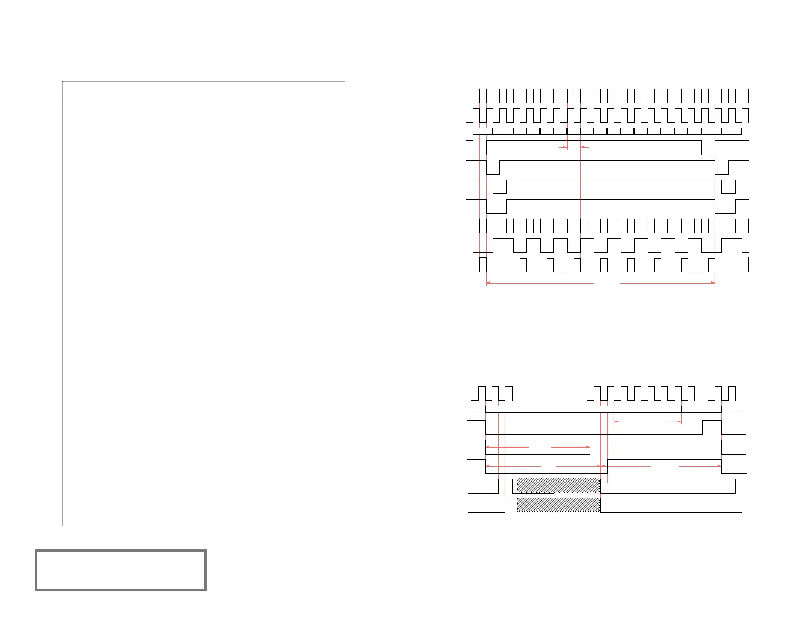
Shown is a full 16-bit microcode cycle, as defined by RCK (ROM clock). The number of pulses of SCK (bit-shift clock) within
an RCK cycle, and hence the high period of RCK, is variable from 1 to 16, as determined by the binary code presented by
microcode bits CC0,1,2,3.
This is an idealised presentation of the timing relationships, the real-world edge relationships will differ somewhat.
Measured values:
MCK high=60 ns, low=65nS
RCK low=180nS, lagging MCK –edge by 40nS
In each refresh cycle, 32 memory access cycles are performed, one for each row in the 1103s. The refresh memory access
cycles each require 5 MCK cycles. An additional MCK cycle is needed to transition into the refresh period, thus:
refresh period = (1+ 32*5 ) * 125nS = 20.125µS.
The run period is determined by the refresh delay monostable, so varies with RC tolerances. The calculated design target for
the monostable is 820µS. This will be rounded out to allow completion of an RCK cycle. Each refresh cycle only refreshes
half the RAM memory banks however, with a given bank being refreshed on alternate cycles. The effective refresh rate is
approximately:
refresh rate = 2 * (820 + 20) = 1680µS, or 595 Hz.