Do you have a question about the HP 9830 and is the answer not in the manual?
Provides a high-level overview of the HP 9830 computer system architecture and major components.
Details the 8.000 MHz clock generation and I/O circuitry for the CPU.
Illustrates microcode sequencing, controls, and register operations.
Details the Binary ALU, BCD ALU, and associated carry logic.
Covers M/T registers, memory cycle generation, and bus operations.
Details ROM bank selection, addressing, ROM cards, cartridges, and basic ROM.
Illustrates RAM bank selection, addressing, and the 4KW RAM array.
Details the I/O state machine, flag sense, and I/O controls.
Covers keyboard logic, scan, interconnect, and key data control.
Details display logic, column decoders, and character display circuitry.
Covers tape interface, command decode, drive control, data clock, and read/write operations.
Shows the power supply circuitry, including voltage regulation and filtering components.
Includes IC units list, types, calculations, signal names, memory map, and timing diagrams.
Shows the physical layout of the backplane, indicating connector positions and board locations.
Illustrates the physical layout of CPU, Memory, I/O, Display, Keyboard, Tape, and Power Supply boards.
| Model | 9830 |
|---|---|
| Category | Desktop |
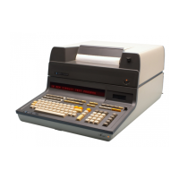
| Release Year | 1972 |
| Memory (Base) | 4 KB |
| Display Type | LED |
| Display (Characters per line) | 32 |
| Programming Language | BASIC |
| Type | Programmable Calculator |
| Memory | 4 KB |
| Display | LED |
| Manufacturer | Hewlett Packard |
| CPU | Custom HP |
| Processor | Custom HP |
| Word Size | 16 bits |