4 - 2
The signals from the RX band swtiching circuits are then
applied to the left side displayed 1st mixer circuit (IC1005, pin
6).
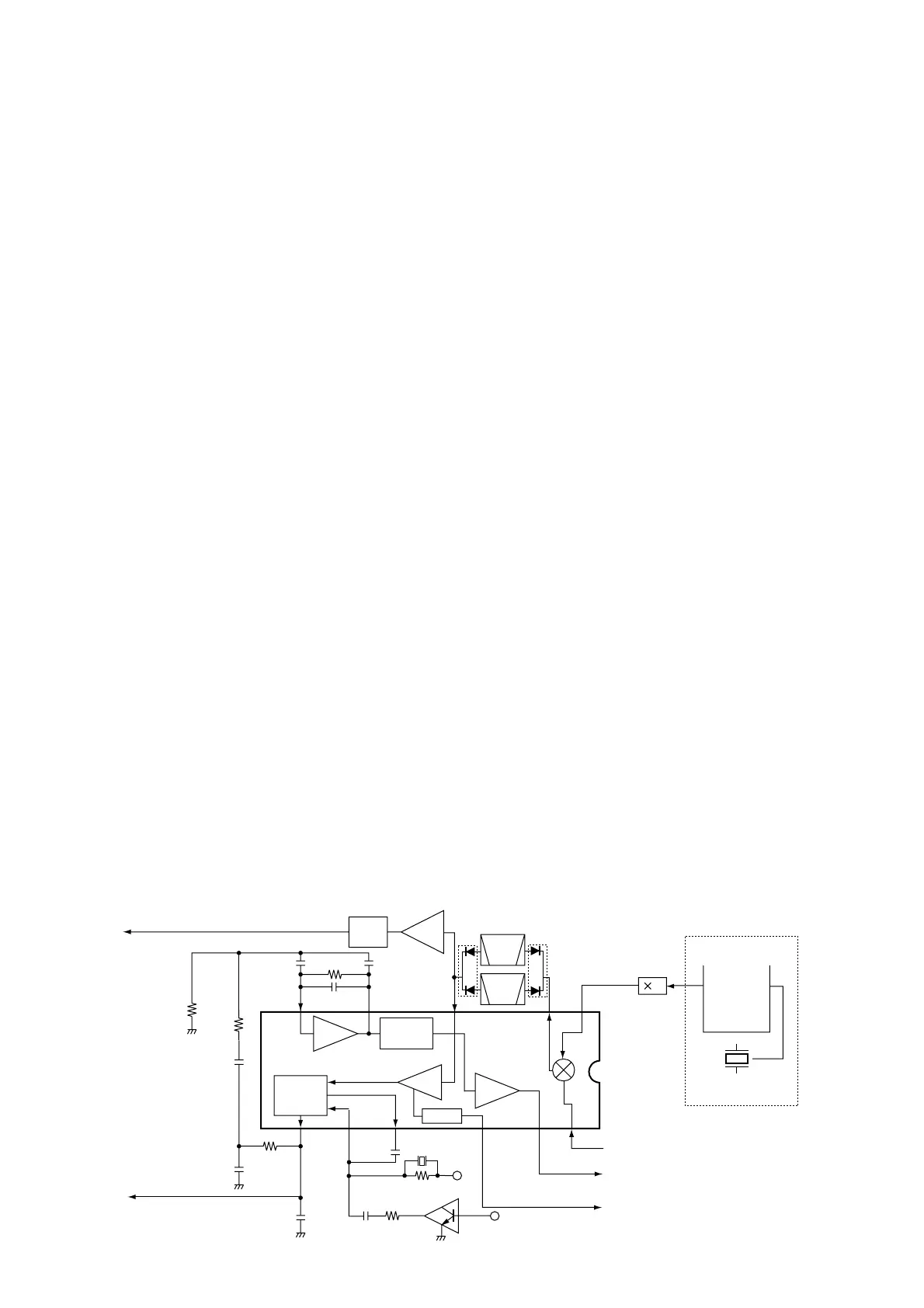
4-1-3 1ST MIXER AND 1ST IF CIRCUIT FOR LEFT
SIDE DISPLAY (MAIN UNIT)
The 1st mixer circuit converts the received RF signals to a
fixed frequency of the 1st IF signal with a PLL output fre-
quency. By changing the PLL frequency, only the desired fre-
quency will pass through the bandpass filter at the next stage
of 1st mixer circuit.
The RF signals are mixed with 1st LO signals at the 1st mixer
(IC1005) to produce a 38.85 MHz 1st IF signal. The 1st IF
signal is output from pin 1, and passed through the crystal
bandpass filter (FI1003) to suppress unwanted harmonic
components. The filtered signal is amplified at the IF amplifi-
er (Q1040) after being passed through the limiter circuit
(D1021). The amplified signal is applied to the 2nd mixer cir-
cuit (IC1001).
4-1-4 2ND IF AND DEMODULATOR CIRCUITS FOR
LEFT SIDE DISPLAY (MAIN UNIT)
The 2nd mixer circuit converts the 1st IF signal to a 2nd IF
signal. A double conversion superheterodyne system (which
converts receive signal twice) improves the image rejection
ratio and obtains stable receiver gain.
The FM IC IC (IC1001) contains the 2nd mixer, limiter and
noise amplifiers, quadrature detector, S-meter detector,
active filter circuits, etc. A 2nd LO signal (38.4 MHz) is pro-
duced at the PLL circuit by dividing it’s reference frequency.
The 38.85 MHz 1st IF signal from the IF amplifier (Q1040) is
applied to the 2nd mixer section of the FM IF IC (IC1001, pin
16), and is mixed with the 2nd LO signal (38.4 MHz) to be
converted to a 450 kHz 2nd IF signal.
The 2nd IF signal is applied to the each demodulator circuits
by AM or FM mode.
• FM MODE
The 2nd IF signal is output from the FM IF IC (IC1001, pin 3)
and passes through the ceramic bandpass filter (FI1001).
The filtered signal is fed back to the IC, and amplified at the
limiter amplifier section (pin 5), then demodulated into AF sig-
nals at the quadrature detector section (pins 10, 11). The
detected AF signals are output from pin 9 and are applied to
the AF circuit via the AM/FM selector circuit (IC2015, pins 7,
1).
• AM MODE
The 2nd IF signal is output from the FM IF IC (IC1001, pin 3)
and passes through the ceramic bandpass filter (FI1000).
The filtered signal is applied to the AM detector circuit
(Q1017) to convert into AF signals, and then amplified at the
Q1014 (pins 5, 1). The amplified AF signals are applied to the
AF circuit via the AM/FM selector circuit (IC2015, pins 6, 1).
4-1-5 AF AMPLIFIER CIRCUIT FOR LEFT SIDE
DISPLAY (MAIN UNIT)
The AF amplifier circuit amplifies the demodulated AF signals
to drive a speaker.
The AF signals pass through the AF mute switch (Q1010),
and are then applied to the electric volume control circuit
(IC2011, pin 1) as “VAFO” signal after being passed through
the low-pass filter (Q1007). The level controlled AF signals
are output from pin 2, and are then applied to the AF power
amplifier (IC2012, pin 2) via the “VOUT1” signal. The power
amplified AF signals are applied to the internal speaker (SP1)
via the [EXT SP] jack (J2005).
The electronic volume control circuit controls AF gain, there-
fore, the AF output level is according to the [VOL] setting and
also the squelch conditions.
4-1-6 NOISE SQUELCH CIRCUIT FOR LEFT SIDE
DISPLAY (MAIN UNIT)
• NOISE SQUELCH
A noise squelch circuit cuts out AF signals when no RF sig-
nal is received. By detecting noise components in the AF sig-
nal, the squelch circuit switches the AF mute switch.